- 您现在的位置:买卖IC网 > PDF目录16425 > AD9983A/PCBZ (Analog Devices Inc)KIT EVALUATION AD9983A PDF资料下载
参数资料
| 型号: | AD9983A/PCBZ |
| 厂商: | Analog Devices Inc |
| 文件页数: | 11/44页 |
| 文件大小: | 0K |
| 描述: | KIT EVALUATION AD9983A |
| 标准包装: | 1 |
| 系列: | Advantiv® |
| 主要目的: | 视频,视频处理 |
| 嵌入式: | 否 |
| 已用 IC / 零件: | AD9983A |
| 主要属性: | 3 x 8-Bit 140 MSPS ADC's |
| 次要属性: | 集成式 PLL 和 VCO |
| 已供物品: | 板 |
第1页第2页第3页第4页第5页第6页第7页第8页第9页第10页当前第11页第12页第13页第14页第15页第16页第17页第18页第19页第20页第21页第22页第23页第24页第25页第26页第27页第28页第29页第30页第31页第32页第33页第34页第35页第36页第37页第38页第39页第40页第41页第42页第43页第44页
AD9983A
Rev. 0 | Page 19 of 44
DATAIN
P0
P1
P2
P5
P3
P4
P9
P6
P8
P10
P11
P7
HSYNCx
DATACK
8 CLOCK CYCLE DELAY
DATAOUT
P0
P1
P2
P3
2 CLOCK CYCLE DELAY
HSOUT
06
47
5-
00
8
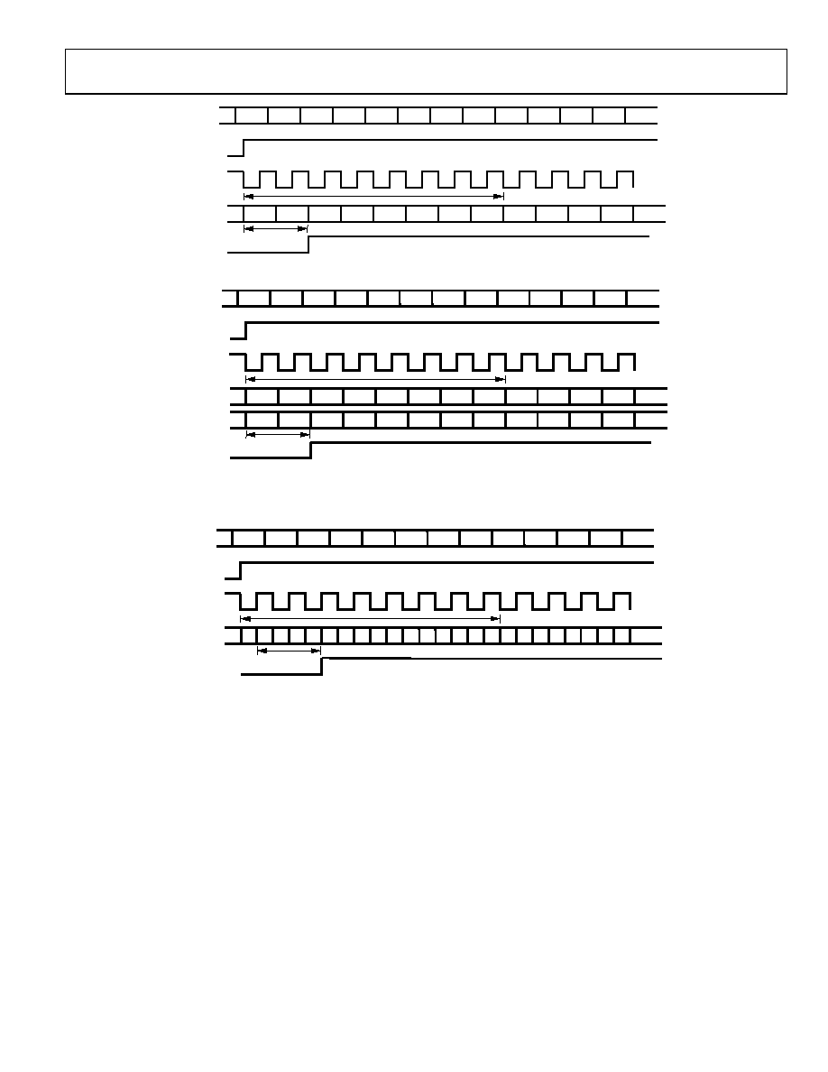
Figure 14. 4:4:4 Timing Mode
DATAIN
P0
P1
P2
P5
P3
P4
P9
P6
P8
P10
P11
P7
HSYNCx
DATACK
8 CLOCK CYCLE DELAY
CB/CROUT
CB0
CR0
CB2
CR2
YOUT
Y0
Y1
Y2
Y3
2 CLOCK CYCLE DELAY
NOTES
1. PIXEL AFTER HSOUT CORRESONDS TO BLUE INPUT.
2. EVEN NUMBER OF PIXEL DELAY BETWEEN HSOUT AND DATAOUT.
HSOUT
06
47
5-
0
09
Figure 15. 4:2:2 Timing Mode
DATAIN
P0
P1
P2
P5
P3
P4
P9
P6
P8
P10
P11
P7
HSYNCx
DATACK
8 CLOCK CYCLE DELAY
2 CLOCK CYCLE DELAY
DDR NOTES
1. OUTPUT DATACK MAY BE DELAYED 1/4 CLOCK PERIOD IN THE REGISTERS.
2. SEE PROJECT DOCUMENT FOR VALUES OF F (FALLING EDGE) AND R (RISING EDGE).
3. FOR DDR 4:2:2 MODE: TIMING IS IDENTICAL, VALUES OF F AND R CHANGE.
GENERAL NOTES
1. DATA DELAY MAY VARY ± ONE CLOCK CYCLE, DEPENDING ON PHASE SETTING.
2. ADCs SAMPLE INPUT ON FALLING EDGE OF DATACK.
3. HSYNC SHOWN IS ACTIVE HIGH (EDGE SHOWN IS LEADING EDGE).
HSOUT
064
75
-010
F0 R0 F1 R1 F2 R2 F3 R3
Figure 16. Double Data Rate (DDR) Timing Mode
HSYNC TIMING
The Hsync is processed in the AD9983A to eliminate ambiguity
in the timing of the leading edge with respect to the phase-
delayed pixel clock and data.
The Hsync input is used as a reference to generate the pixel
sampling clock. The sampling phase can be adjusted with
respect to Hsync through a full 360° in 32 steps via the phase
adjust register (to optimize the pixel sampling time). Display
systems use Hsync to align memory and display write cycles, so
it is important to have a stable timing relationship between
Hsync output (HSOUT) and the data clock (DATACK).
Three things happen to Hsync in the AD9983A. First, the
polarity of Hsync input is determined and thus has a known
output polarity. The known output polarity can be programmed
either active high or active low (Register 0x12, Bit 3). Second,
HSOUT is aligned with DATACK and data outputs. Third, the
duration of HSOUT (in pixel clocks) is set via Register 0x13.
HSOUT is the sync signal that should be used to drive the rest
of the display system.
相关PDF资料 |
PDF描述 |
|---|---|
| VI-J43-EX | CONVERTER MOD DC/DC 24V 75W |
| GBC15DREN-S93 | CONN EDGECARD 30POS .100 EYELET |
| S01-01-R | SOLDER SLEEVE IMMERS RESIS .650" |
| UPA1A102MPD6TD | CAP ALUM 1000UF 10V 20% RADIAL |
| H3AAH-6436G | IDC CABLE - HSC64H/AE64G/HSC64H |
相关代理商/技术参数 |
参数描述 |
|---|---|
| AD9983KSTZ-110 | 制造商:Rochester Electronics LLC 功能描述: 制造商:Analog Devices 功能描述: |
| AD9983KSTZ-140 | 制造商:Rochester Electronics LLC 功能描述: 制造商:Analog Devices 功能描述: |
| AD9983KSTZ-170 | 制造商:Rochester Electronics LLC 功能描述:- Bulk 制造商:Analog Devices 功能描述: |
| AD9984A | 制造商:AD 制造商全称:Analog Devices 功能描述:High Performance 10-Bit Display Interface |
| AD9984A/PCB | 制造商:Analog Devices 功能描述:DISPLAY INTRFC - Bulk |
发布紧急采购,3分钟左右您将得到回复。