- 您现在的位置:买卖IC网 > PDF目录378277 > ADC081500CIYB (NATIONAL SEMICONDUCTOR CORP) High Performance, Low Power, 8-Bit, 1.5 GSPS A/D Converter PDF资料下载
参数资料
| 型号: | ADC081500CIYB |
| 厂商: | NATIONAL SEMICONDUCTOR CORP |
| 元件分类: | ADC |
| 英文描述: | High Performance, Low Power, 8-Bit, 1.5 GSPS A/D Converter |
| 中文描述: | 1-CH 8-BIT PROPRIETARY METHOD ADC, PARALLEL ACCESS, PQFP128 |
| 封装: | MS-026BFB, LQFP-128 |
| 文件页数: | 10/28页 |
| 文件大小: | 830K |
| 代理商: | ADC081500CIYB |
第1页第2页第3页第4页第5页第6页第7页第8页第9页当前第10页第11页第12页第13页第14页第15页第16页第17页第18页第19页第20页第21页第22页第23页第24页第25页第26页第27页第28页
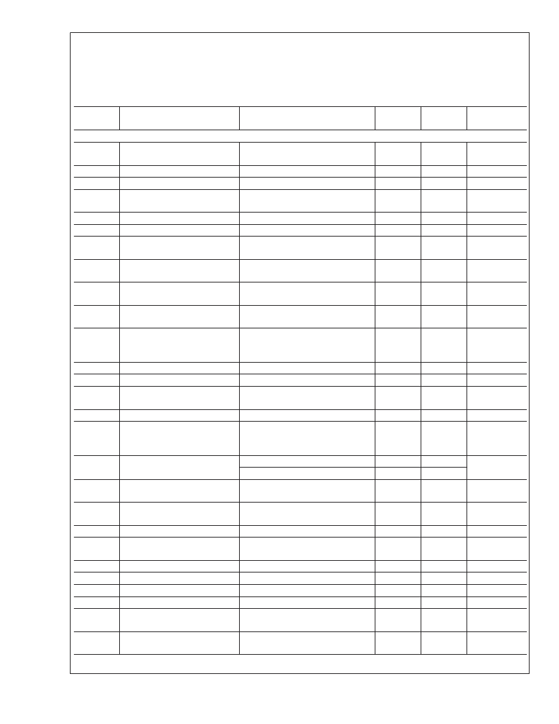
Converter Electrical Characteristics
(Continued)
The following specifications apply after calibration for V
= V
= +1.9V
, OutV = 1.9V, V
(a.c. coupled) Full Scale Range =
differential 870mV
, C
= 10 pF, Differential (a.c. coupled) sinewave input clock, f
CLK
= 1.5 GHz at 0.5V
with 50% duty
cycle, V
= Floating, Normal Control Mode, Single Data Rate Mode, R
= 3300
0.1%, Analog Signal Source Impedance
= 100
Differential.
Boldface limits apply for T
A
= T
MIN
to T
MAX
. All other limits T
A
= 25C, unless otherwise noted. (Notes 6,
7)
Symbol
Parameter
Conditions
Typical
(Note 8)
Limits
(Note 8)
Units
(Limits)
AC ELECTRICAL CHARACTERISTICS
Input Clock Duty Cycle
200 MHz
≤
Input clock frequency
≤
1.5 GHz (Note 12)
(Note 11)
(Note 11)
50
20
80
133
133
45
55
% (min)
% (max)
ps (min)
ps (min)
% (min)
% (max)
ps
ps
t
CL
t
CH
Input Clock Low Time
Input Clock High Time
333
333
DCLK Duty Cycle
(Note 11)
50
t
RS
t
RH
Reset Setup Time
Reset Hold Time
Syncronizing Edge to DCLK
Output Delay
(Note 11)
(Note 11)
f
CLKIN
= 1.5 GHz
f
CLKIN
= 200 MHz
150
250
3.53
3.85
t
SD
ns
t
RPW
Reset Pulse Width
(Note 11)
4
Clock Cycles
(min)
t
LHT
Differential Low to High
Transition Time
Differential High to Low
Transition Time
10% to 90%, C
L
= 2.5 pF
250
ps
t
HLT
10% to 90%, C
L
= 2.5 pF
250
ps
t
OSK
DCLK to Data Output Skew
50% of DCLK transition to 50% of
Data transition, SDR Mode
and DDR Mode, 0 DCLK (Note 11)
DDR Mode, 90 DCLK (Note 11)
DDR Mode, 90 DCLK (Note 11)
Input CLK+ Fall to Acquisition of
Data
±
50
ps (max)
t
SU
t
H
Data to DCLK Set-Up Time
DCLK to Data Hold Time
1
1
ns
ns
t
AD
Sampling (Aperture) Delay
1.3
ns
t
AJ
Aperture Jitter
Input Clock to Data Output
Delay (in addition to Pipeline
Delay)
Pipeline Delay (Latency)
(Notes 11, 14)
0.4
ps rms
t
OD
50% of Input Clock transition to 50%
of Data transition
3.1
ns
D Outputs
Dd Outputs
Differential V
IN
step from
±
1.2V to
0V to get accurate conversion
13
14
Input Clock
Cycles
Input Clock
Cycle
Over Range Recovery Time
1
t
WU
PD low to Rated Accuracy
Conversion (Wake-Up Time)
Serial Clock Frequency
Data to Serial Clock Setup
Time
Data to Serial Clock Hold Time
Serial Clock Low Time
Serial Clock High Time
Calibration Cycle Time
500
ns
f
SCLK
(Note 11)
100
MHz
t
SSU
(Note 11)
2.5
ns (min)
t
SH
(Note 11)
1
ns (min)
ns (min)
ns (min)
Clock Cycles
Clock Cycles
(min)
Clock Cycles
(min)
4
4
t
CAL
1.4 x 10
5
t
CAL_L
CAL Pin Low Time
See
Figure 9
(Note 11)
80
t
CAL_H
CAL Pin High Time
See
Figure 9
(Note 11)
80
A
www.national.com
10
相关PDF资料 |
PDF描述 |
|---|---|
| ADC081500EVAL | High Performance, Low Power, 8-Bit, 1.5 GSPS A/D Converter |
| ADC08161 | 500 ns A/D Converter with S/H Function and 2.5V Bandgap Reference(500ns带S/H功能和2.5V带隙参考的A/D转换器) |
| ADC08161CIWM | 500 ns A/D Converter with S/H Function and 2.5V Bandgap Reference |
| ADC0816 | 8-BitμP Compatible A/D Converters with 16-Channel Multiplexer(带16通道多路器的8位μP兼容A/D转换器) |
| ADC0817 | 8-BitμP Compatible A/D Converters with 16-Channel Multiplexer(带16通道多路器的8位μP兼容A/D转换器) |
相关代理商/技术参数 |
参数描述 |
|---|---|
| ADC081500CIYB/NOPB | 功能描述:模数转换器 - ADC RoHS:否 制造商:Texas Instruments 通道数量:2 结构:Sigma-Delta 转换速率:125 SPs to 8 KSPs 分辨率:24 bit 输入类型:Differential 信噪比:107 dB 接口类型:SPI 工作电源电压:1.7 V to 3.6 V, 2.7 V to 5.25 V 最大工作温度:+ 85 C 安装风格:SMD/SMT 封装 / 箱体:VQFN-32 |
| ADC081500DEV | 制造商:NSC 制造商全称:National Semiconductor 功能描述:High Performance, Low Power, 8-Bit, 1.5 GSPS A/D Converter |
| ADC081500EVAL | 制造商:NSC 制造商全称:National Semiconductor 功能描述:High Performance, Low Power, 8-Bit, 1.5 GSPS A/D Converter |
| ADC0816 | 制造商:NSC 制造商全称:National Semiconductor 功能描述:8-Bit レP Compatible A/D Converters with 16-Channel Multiplexer |
| ADC0816_07 | 制造商:NSC 制造商全称:National Semiconductor 功能描述:8-Bit レP Compatible A/D Converters with 16-Channel Multiplexer |
发布紧急采购,3分钟左右您将得到回复。