- 您现在的位置:买卖IC网 > PDF目录378277 > ADC081500CIYB (NATIONAL SEMICONDUCTOR CORP) High Performance, Low Power, 8-Bit, 1.5 GSPS A/D Converter PDF资料下载
参数资料
| 型号: | ADC081500CIYB |
| 厂商: | NATIONAL SEMICONDUCTOR CORP |
| 元件分类: | ADC |
| 英文描述: | High Performance, Low Power, 8-Bit, 1.5 GSPS A/D Converter |
| 中文描述: | 1-CH 8-BIT PROPRIETARY METHOD ADC, PARALLEL ACCESS, PQFP128 |
| 封装: | MS-026BFB, LQFP-128 |
| 文件页数: | 19/28页 |
| 文件大小: | 830K |
| 代理商: | ADC081500CIYB |
第1页第2页第3页第4页第5页第6页第7页第8页第9页第10页第11页第12页第13页第14页第15页第16页第17页第18页当前第19页第20页第21页第22页第23页第24页第25页第26页第27页第28页
1.0 Functional Description
(Continued)
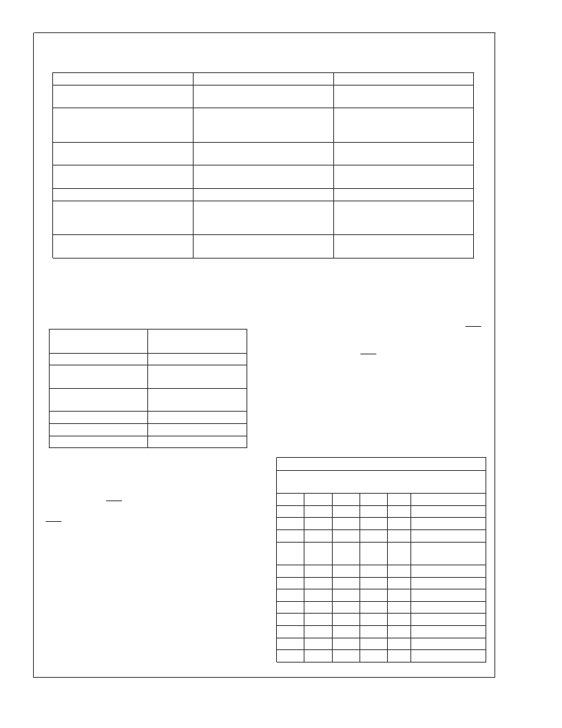
TABLE 1. Features and modes
Feature
Normal Control Mode
Extended Control Mode
Selected with DE bit in the
Configuration Register
Selected with DCP bit in the
Configuration Register. See
Section
1.4 REGISTER DESCRIPTION
Selected with the OE bit in the
Configuration Register
Selected with the OV bit (9)in the
Configuration Register
Short delay only.
Up to 512 step adjustments over a
nominal range of 560 mV to 840 mV.
Selected using register 3h.
±
45 mV adjustments in 512 steps
using register 2h.
SDR or DDR Clocking
Selected with pin 4
DDR Clock Phase
Not Selectable (0 Phase Only)
SDR Data transitions with rising or
falling DCLK edge
Selected with pin 4
LVDS output level
Selected with pin 3
Power-On Calibration Delay
Delay Selected with pin 127
Full-Scale Range
Options (650 mV
P-P
or 870 mV
P-P
)
selected with pin 14.
Input Offset Adjust
Not possible
The default state of the Extended Control Mode is set upon
power-on reset (internally performed by the device) and is
shown in
Table 2
.
TABLE 2. Extended Control Mode Operation (Pin 14
Floating)
Feature
Extended Control Mode
Default State
DDR Clocking
Data changes with DCLK
edge (0 phase)
Normal amplitude
(710 mV
P-P
)
Short Delay
700 mV nominal
No adjustment
SDR or DDR Clocking
DDR Clock Phase
LVDS Output Amplitude
Calibration Delay
Full-Scale Range
Input Offset Adjust
1.3 THE SERIAL INTERFACE
The 3-pin serial interface is enabled only when the device is
in the Extended Control mode. The pins of this interface are
Serial Clock (SCLK), Serial Data (SDATA) and Serial Inter-
face Chip Select (SCS) Three write only registers are acces-
sible through this serial interface.
SCS:
This signal should be asserted low while accessing a
register through the serial interface. Setup and hold times
with respect to the SCLK must be observed.
SCLK
: Serial data input is accepted with the rising edge of
this signal.
SDATA:
Each register access requires a specific 32-bit pat-
tern at this input. This pattern consists of a header, register
address and register value. The data is shifted in MSB first.
Setup and hold times with respect to the SCLK must be
observed. See the Timing Diagram.
Each Register access consists of 32 bits, as shown in
Figure
5
of the Timing Diagrams. The fixed header pattern is 0000
0000 0001 (eleven zeros followed by a 1). The loading
sequence is such that a "0" is loaded first. These 12 bits form
the header. The next 4 bits are the address of the register
that is to be written to and the last 16 bits are the data written
to the addressed register. The addresses of the various
registers are indicated in
Table 3
.
Refer to the Register Description (Section 1.4) for informa-
tion on the data to be written to the registers.
Subsequent register accesses may be performed immedi-
ately, starting with the 33rd SCLK. This means that the SCS
input does not have to be de-asserted and asserted again
between register addresses. It is possible, although not rec-
ommended, to keep the SCS input permanently enabled (at
a logic low) when using extended control.
IMPORTANT NOTE:
The Serial Interface should not be
used when calibrating the ADC. Doing so will impair the
performance of the device until it is re-calibrated correctly.
Programming the serial registers will also reduce dynamic
performance of the ADC for the duration of the register
access time.
TABLE 3. Register Addresses
4-Bit Address
Loading Sequence:
A3 loaded after H0, A0 loaded last
A2
A1
A0
0
0
0
0
0
1
0
1
0
0
1
1
A3
0
0
0
0
Hex
0h
1h
2h
3h
Register Addressed
Reserved
Configuration
Input Offset
Input Full-Scale
Voltage Adjust
Reserved
Reserved
Reserved
Reserved
Reserved
Reserved
Reserved
Reserved
0
0
0
0
1
1
1
1
1
1
1
1
0
0
0
0
0
0
1
1
0
0
1
1
0
1
0
1
0
1
0
1
4h
5h
6h
7h
8h
9h
Ah
Bh
A
www.national.com
19
相关PDF资料 |
PDF描述 |
|---|---|
| ADC081500EVAL | High Performance, Low Power, 8-Bit, 1.5 GSPS A/D Converter |
| ADC08161 | 500 ns A/D Converter with S/H Function and 2.5V Bandgap Reference(500ns带S/H功能和2.5V带隙参考的A/D转换器) |
| ADC08161CIWM | 500 ns A/D Converter with S/H Function and 2.5V Bandgap Reference |
| ADC0816 | 8-BitμP Compatible A/D Converters with 16-Channel Multiplexer(带16通道多路器的8位μP兼容A/D转换器) |
| ADC0817 | 8-BitμP Compatible A/D Converters with 16-Channel Multiplexer(带16通道多路器的8位μP兼容A/D转换器) |
相关代理商/技术参数 |
参数描述 |
|---|---|
| ADC081500CIYB/NOPB | 功能描述:模数转换器 - ADC RoHS:否 制造商:Texas Instruments 通道数量:2 结构:Sigma-Delta 转换速率:125 SPs to 8 KSPs 分辨率:24 bit 输入类型:Differential 信噪比:107 dB 接口类型:SPI 工作电源电压:1.7 V to 3.6 V, 2.7 V to 5.25 V 最大工作温度:+ 85 C 安装风格:SMD/SMT 封装 / 箱体:VQFN-32 |
| ADC081500DEV | 制造商:NSC 制造商全称:National Semiconductor 功能描述:High Performance, Low Power, 8-Bit, 1.5 GSPS A/D Converter |
| ADC081500EVAL | 制造商:NSC 制造商全称:National Semiconductor 功能描述:High Performance, Low Power, 8-Bit, 1.5 GSPS A/D Converter |
| ADC0816 | 制造商:NSC 制造商全称:National Semiconductor 功能描述:8-Bit レP Compatible A/D Converters with 16-Channel Multiplexer |
| ADC0816_07 | 制造商:NSC 制造商全称:National Semiconductor 功能描述:8-Bit レP Compatible A/D Converters with 16-Channel Multiplexer |
发布紧急采购,3分钟左右您将得到回复。