- 您现在的位置:买卖IC网 > PDF目录223307 > ADC1113D125HN (NXP Semiconductors N.V.) Dual 11 bits ADC; 125 Msps; serial JESD204A PDF资料下载
参数资料
| 型号: | ADC1113D125HN |
| 厂商: | NXP Semiconductors N.V. |
| 元件分类: | 外设及接口 |
| 英文描述: | Dual 11 bits ADC; 125 Msps; serial JESD204A |
| 封装: | ADC1113D125HN/C1<SOT684-7 (HVQFN56)|<<http://www.nxp.com/packages/SOT684-7.html<1<Always Pb-free,;ADC1113D125HN/C1<SOT684-7 (HVQFN56)|<<http://www.nxp.com/packages/SOT684 |
| 文件页数: | 11/41页 |
| 文件大小: | 536K |
| 代理商: | ADC1113D125HN |
第1页第2页第3页第4页第5页第6页第7页第8页第9页第10页当前第11页第12页第13页第14页第15页第16页第17页第18页第19页第20页第21页第22页第23页第24页第25页第26页第27页第28页第29页第30页第31页第32页第33页第34页第35页第36页第37页第38页第39页第40页第41页
ADC1113D125
All information provided in this document is subject to legal disclaimers.
NXP B.V. 2011. All rights reserved.
Product data sheet
Rev. 3 — 10 February 2011
19 of 41
NXP Semiconductors
ADC1113D125
Dual 11-bit ADC; serial JESD204A interface
Single-ended or differential clock inputs can be selected via the SPI (see Table 20). If
single-ended is selected, the input pin (CLKM or CLKP) is selected via control bit
SE_SEL.
If single-ended is implemented without setting bit SE_SEL accordingly, the unused pin
should be connected to ground via a capacitor.
11.3.3 Clock input divider
The ADC1113D125 contains an input clock divider that divides the incoming clock by a
factor of 2 (when bit CLKDIV2_SEL = logic 1; see Table 20). This feature allows the user
to deliver a higher clock frequency with better jitter performance, leading to a better SNR
result once acquisition has been performed.
11.3.4 Duty cycle stabilizer
The duty cycle stabilizer can improve the overall performances of the ADC by
compensating the input clock signal duty cycle. When the duty cycle stabilizer is active
(bit DCS_EN = logic 1; see Table 20), the circuit can handle signals with duty cycles of
between 30 % and 70 % (typical). When the duty cycle stabilizer is disabled
(DCS_EN = logic 0), the input clock signal should have a duty cycle of between 45 % and
55 %.
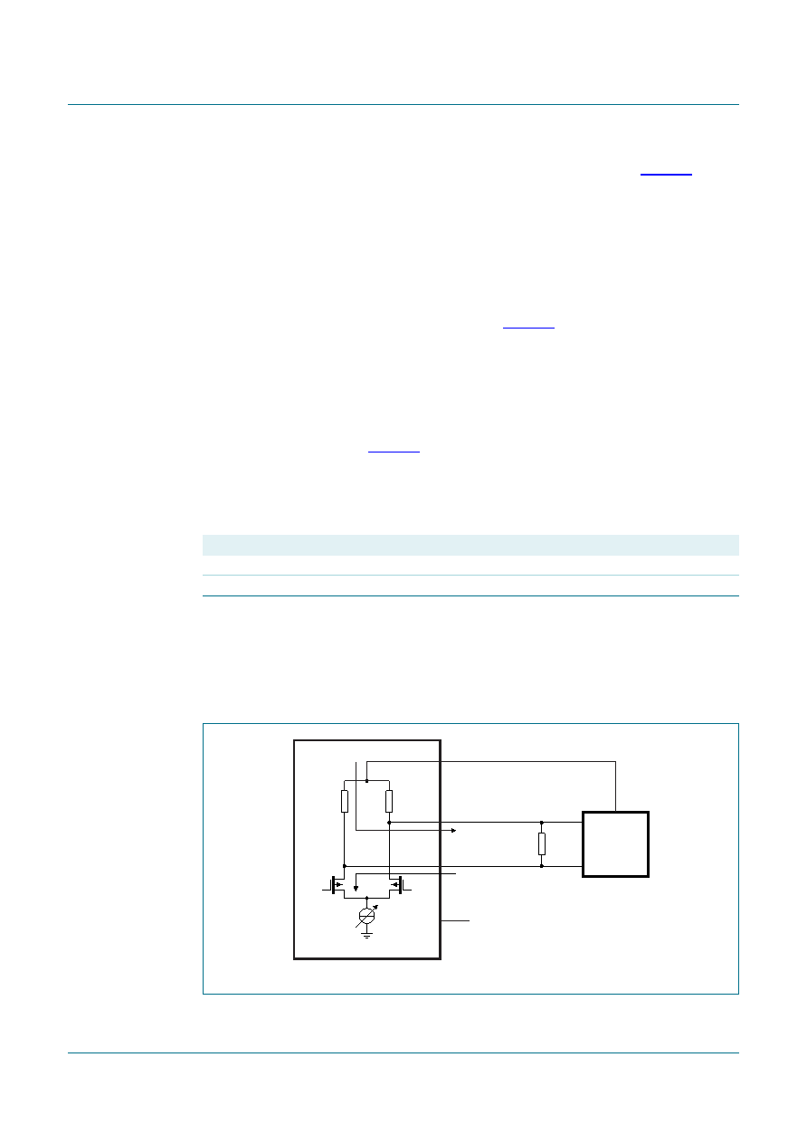
11.4 Digital outputs
11.4.1 Serial output equivalent circuit
The JESD204A standard specifies that if the receiver and the transmitter are DC-coupled,
both must be fed from the same supply.
The output should be terminated when 100
Ω (typical) is reached at the receiver side.
Table 12.
Duty cycle stabilizer
Bit DCS_EN
Description
0
duty cycle stabilizer disable
1
duty cycle stabilizer enable
Fig 19. CML output connection to the receiver (DC-coupled)
VDDD
CMLPA/CLMPB
CMLNA/CLMNB
AGND
005aaa082
12 mA to 26 mA
100
Ω
+
RECEIVER
50
Ω
相关PDF资料 |
PDF描述 |
|---|---|
| ADC1113D125W1 | |
| ADC1113S125HN | Single 11 bits ADC; 125Msps; serial JESD204A |
| ADC1213D065HN | Dual 12-bit ADC; 65 Msps |
| ADD223AB7 | FIBER OPTIC ADD/DROP MUX/DEMUX, LC/UPC CONNECTOR |
| ADE-ED7795/1+ | 100 MHz - 1536 MHz RF/MICROWAVE DOUBLE BALANCED MIXER |
相关代理商/技术参数 |
参数描述 |
|---|---|
| ADC1113D125HN/C1 | 制造商:PHILIPS 制造商全称:NXP Semiconductors 功能描述:Dual 11-bit ADC; serial JESD204A interface |
| ADC1113D125HN/C1,5 | 功能描述:模数转换器 - ADC DUAL 11b ADC 125MSPS RoHS:否 制造商:Texas Instruments 通道数量:2 结构:Sigma-Delta 转换速率:125 SPs to 8 KSPs 分辨率:24 bit 输入类型:Differential 信噪比:107 dB 接口类型:SPI 工作电源电压:1.7 V to 3.6 V, 2.7 V to 5.25 V 最大工作温度:+ 85 C 安装风格:SMD/SMT 封装 / 箱体:VQFN-32 |
| ADC1113D125HNC1 | 制造商:PHILIPS 制造商全称:NXP Semiconductors 功能描述:Dual 11-bit ADC; serial JESD204A interface |
| ADC1113D125HN-C1 | 功能描述:模数转换器 - ADC RoHS:否 制造商:Texas Instruments 通道数量:2 结构:Sigma-Delta 转换速率:125 SPs to 8 KSPs 分辨率:24 bit 输入类型:Differential 信噪比:107 dB 接口类型:SPI 工作电源电压:1.7 V to 3.6 V, 2.7 V to 5.25 V 最大工作温度:+ 85 C 安装风格:SMD/SMT 封装 / 箱体:VQFN-32 |
发布紧急采购,3分钟左右您将得到回复。