参数资料
| 型号: | ADF4351BCPZ |
| 厂商: | Analog Devices Inc |
| 文件页数: | 3/28页 |
| 文件大小: | 0K |
| 描述: | IC SYNTH PLL VCO 32LFCSP |
| 标准包装: | 1 |
| 类型: | 扇出配送,分数-N,整数-N,时钟/频率合成器(RF) |
| PLL: | 是 |
| 输入: | CMOS,TTL |
| 输出: | 时钟 |
| 电路数: | 1 |
| 比率 - 输入:输出: | 1:3 |
| 差分 - 输入:输出: | 无/无 |
| 频率 - 最大: | 4.4GHz |
| 除法器/乘法器: | 是/是 |
| 电源电压: | 3 V ~ 3.6 V |
| 工作温度: | -40°C ~ 85°C |
| 安装类型: | 表面贴装 |
| 封装/外壳: | 32-VFQFN 裸露焊盘,CSP |
| 供应商设备封装: | 32-LFCSP(5x5) |
| 包装: | 托盘 |
第1页第2页当前第3页第4页第5页第6页第7页第8页第9页第10页第11页第12页第13页第14页第15页第16页第17页第18页第19页第20页第21页第22页第23页第24页第25页第26页第27页第28页
Data Sheet
ADF4351
Rev. 0 | Page 11 of 28
CIRCUIT DESCRIPTION
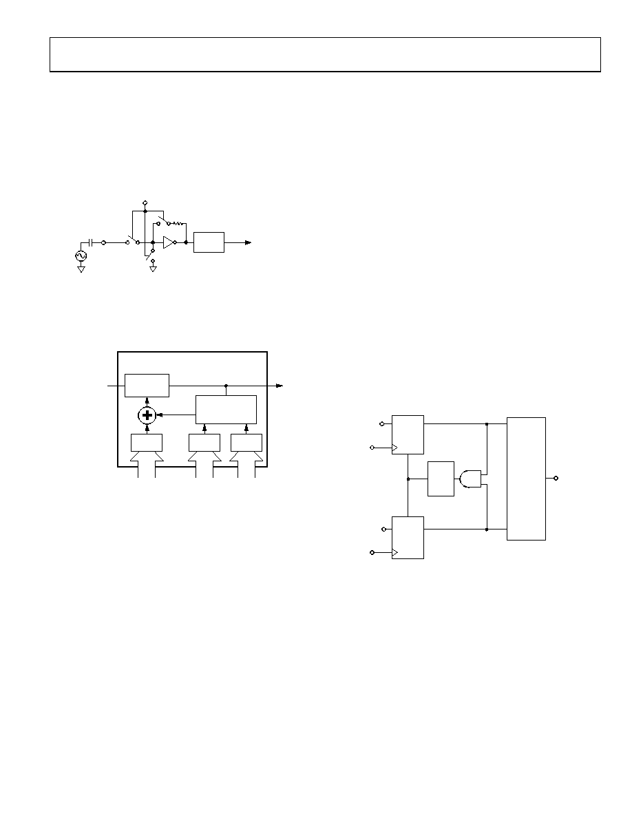
REFERENCE INPUT SECTION
The reference input stage is shown in Figure 16. The SW1 and
SW2 switches are normally closed. The SW3 switch is normally
open. When power-down is initiated, SW3 is closed, and SW1
and SW2 are opened. In this way, no loading of the REFIN pin
occurs during power-down.
BUFFER
TO R COUNTER
REFIN
100k
NC
SW2
SW3
NO
NC
SW1
POWER-DOWN
CONTROL
09800-
005
Figure 16. Reference Input Stage
RF N DIVIDER
The RF N divider allows a division ratio in the PLL feedback
path. The division ratio is determined by the INT, FRAC, and
MOD values, which build up this divider (see Figure 17).
THIRD-ORDER
FRACTIONAL
INTERPOLATOR
MOD
VALUE
FRAC
VALUE
INT
VALUE
RF N DIVIDER
N = INT + FRAC/MOD
FROM
VCO OUTPUT/
OUTPUT DIVIDERS
TO PFD
N COUNTER
09800-
006
Figure 17. RF N Divider
INT, FRAC, MOD, and R Counter Relationship
The INT, FRAC, and MOD values, in conjunction with the
R counter, make it possible to generate output frequencies that
are spaced by fractions of the PFD frequency. For more informa-
tion, see the RF Synthesizer—A Worked Example section.
The RF VCO frequency (RFOUT) equation is
RFOUT = fPFD × (INT + (FRAC/MOD))
(1)
where:
RFOUT is the output frequency of the voltage controlled oscillator
(VCO).
INT is the preset divide ratio of the binary 16-bit counter (23 to
65,535 for the 4/5 prescaler; 75 to 65,535 for the 8/9 prescaler).
FRAC is the numerator of the fractional division (0 to MOD 1).
MOD is the preset fractional modulus (2 to 4095).
The PFD frequency (fPFD) equation is
fPFD = REFIN × [(1 + D)/(R × (1 + T))]
(2)
where:
REFIN is the reference input frequency.
D is the REFIN doubler bit (0 or 1).
R is the preset divide ratio of the binary 10-bit programmable
reference counter (1 to 1023).
T is the REFIN divide-by-2 bit (0 or 1).
Integer-N Mode
If FRAC = 0 and the DB8 (LDF) bit in Register 2 is set to 1, the
synthesizer operates in integer-N mode. The DB8 bit in Register 2
should be set to 1 for integer-N digital lock detect.
R Counter
The 10-bit R counter allows the input reference frequency
(REFIN) to be divided down to produce the reference clock
to the PFD. Division ratios from 1 to 1023 are allowed.
PHASE FREQUENCY DETECTOR (PFD) AND
CHARGE PUMP
The phase frequency detector (PFD) takes inputs from the
R counter and N counter and produces an output proportional
to the phase and frequency difference between them. Figure 18
is a simplified schematic of the phase frequency detector.
U3
CLR2
Q2
D2
U2
DOWN
UP
HIGH
CPOUT
–IN
+IN
CHARGE
PUMP
DELAY
CLR1
Q1
D1
U1
09800-
007
Figure 18. PFD Simplified Schematic
The PFD includes a programmable delay element that sets the
width of the antibacklash pulse (ABP). This pulse ensures that
there is no dead zone in the PFD transfer function. Bit DB22 in
Register 3 (R3) is used to set the ABP as follows:
When Bit DB22 is set to 0, the ABP width is programmed to
6 ns, the recommended value for fractional-N applications.
When Bit DB22 is set to 1, the ABP width is programmed to
3 ns, the recommended value for integer-N applications.
For integer-N applications, the in-band phase noise is improved
by enabling the shorter pulse width. The PFD frequency can
operate up to 90 MHz in this mode. To operate with PFD
frequencies higher than 45 MHz, VCO band select must be dis-
abled by setting the phase adjust bit (DB28) to 1 in Register 1.
相关PDF资料 |
PDF描述 |
|---|---|
| ADF4360-0BCPZRL7 | IC SYNTHESIZER VCO 24LFCSP |
| ADF4360-1BCPZRL7 | IC SYNTHESIZER VCO 24LFCSP |
| ADF4360-2BCPZRL7 | IC SYNTHESIZER VCO 24LFCSP |
| ADF4360-3BCPZRL7 | IC SYNTHESIZER VCO 24LFCSP |
| ADF4360-4BCPZRL7 | IC SYNTHESIZER VCO 24LFCSP |
相关代理商/技术参数 |
参数描述 |
|---|---|
| ADF4351BCPZ-RL7 | 功能描述:IC SYNTH PLL VCO 32LFCSP RoHS:是 类别:集成电路 (IC) >> 时钟/计时 - 时钟发生器,PLL,频率合成器 系列:- 标准包装:2,000 系列:- 类型:PLL 时钟发生器 PLL:带旁路 输入:LVCMOS,LVPECL 输出:LVCMOS 电路数:1 比率 - 输入:输出:2:11 差分 - 输入:输出:是/无 频率 - 最大:240MHz 除法器/乘法器:是/无 电源电压:3.135 V ~ 3.465 V 工作温度:0°C ~ 70°C 安装类型:表面贴装 封装/外壳:32-LQFP 供应商设备封装:32-TQFP(7x7) 包装:带卷 (TR) |
| ADF4351BCPZ-U5 | 制造商:Analog Devices 功能描述:- Rail/Tube |
| ADF4351BCPZ-U6 | 制造商:Analog Devices 功能描述:WIDEBAND SYNTHESIZER WITH INTEGRATED VCO - Rail/Tube |
| ADF4355-2BCPZ | 功能描述:IC INTEGRATED SYNTH/VCO 32LFCSP 制造商:analog devices inc. 系列:- 包装:托盘 零件状态:有效 类型:* PLL:是 输入:时钟 输出:时钟 电路数:1 比率 - 输入:输出:1:2 差分 - 输入:输出:无/无 频率 - 最大值:4.4GHz 分频器/倍频器:是/是 电压 - 电源:3.15 V ~ 3.45 V 工作温度:-40°C ~ 85°C 安装类型:表面贴装 封装/外壳:32-WFQFN 裸露焊盘,CSP 供应商器件封装:32-LFCSP-WQ(5x5) 标准包装:1 |
| ADF4355-2BCPZ-RL7 | 功能描述:IC INTEGRATED SYNTH/VCO 32LFCSP 制造商:analog devices inc. 系列:- 包装:带卷(TR) 零件状态:有效 类型:* PLL:是 输入:时钟 输出:时钟 电路数:1 比率 - 输入:输出:1:2 差分 - 输入:输出:无/无 频率 - 最大值:4.4GHz 分频器/倍频器:是/是 电压 - 电源:3.15 V ~ 3.45 V 工作温度:-40°C ~ 85°C 安装类型:表面贴装 封装/外壳:32-WFQFN 裸露焊盘,CSP 供应商器件封装:24-LFCSP-WQ(4x4) 标准包装:1,500 |
发布紧急采购,3分钟左右您将得到回复。