- 您现在的位置:买卖IC网 > PDF目录15308 > ADM1066ASUZ-REEL (Analog Devices Inc)IC SEQUENCER/SUPERVISOR 48TQFP PDF资料下载
参数资料
| 型号: | ADM1066ASUZ-REEL |
| 厂商: | Analog Devices Inc |
| 文件页数: | 21/32页 |
| 文件大小: | 0K |
| 描述: | IC SEQUENCER/SUPERVISOR 48TQFP |
| 标准包装: | 2,000 |
| 系列: | Super Sequencer® |
| 类型: | 序列发生器 |
| 监视电压数目: | 12 |
| 输出: | 可编程 |
| 电压 - 阀值: | 可调节/可选择 |
| 工作温度: | -40°C ~ 85°C |
| 安装类型: | 表面贴装 |
| 封装/外壳: | 48-TQFP |
| 供应商设备封装: | 48-TQFP(7x7) |
| 包装: | 带卷 (TR) |
| 配用: | EVAL-ADM1066TQEBZ-ND - BOARD EVALUATION FOR ADM1066TQ |
第1页第2页第3页第4页第5页第6页第7页第8页第9页第10页第11页第12页第13页第14页第15页第16页第17页第18页第19页第20页当前第21页第22页第23页第24页第25页第26页第27页第28页第29页第30页第31页第32页
�� ��
��
��ADM1066�
�VOLTAGE� READBACK�
�The� ADM1066� has� an� on-board,� 12-bit� accurate� ADC� for�
�Table� 9.� ADC� Input� Voltage� Ranges�
�voltage� readback� over� the� SMBus.� The� ADC� has� a� 12-channel�
�analog� mux� on� the� front� end.� The� 12� channels� consist� of� the�
�10� SFD� inputs� (VH,� VPx,� and� VXx)� and� two� auxiliary� (single-�
�SFD� Input�
�Range� (V)�
�0.573� to� 1.375�
�Attenuation�
�Factor�
�1�
�ADC� Input� Voltage�
�Range� (V)�
�0� to� 2.048�
�The� upper� limit� is� the� absolute� maximum� allowed� voltage� on� the� VPx� and�
�ended)� ADC� inputs� (AUX1� and� AUX2).� Any� or� all� of� these�
�inputs� can� be� selected� to� be� read,� in� turn,� by� the� ADC.� The�
�circuit� controlling� this� operation� is� called� the� round-robin�
�circuit.� This� circuit� can� be� selected� to� run� through� its� loop� of�
�conversions� once� or� continuously.� Averaging� is� also� provided�
�for� each� channel.� In� this� case,� the� round-robin� circuit� runs�
�through� its� loop� of� conversions� 16� times� before� returning� a�
�result� for� each� channel.� At� the� end� of� this� cycle,� the� results� are�
�written� to� the� output� registers.�
�The� ADC� samples� single-sided� inputs� with� respect� to� the� AGND�
�pin.� A� 0� V� input� gives� out� Code� 0,� and� an� input� equal� to� the�
�voltage� on� REFIN� gives� out� full� code� (4095� decimal).�
�The� inputs� to� the� ADC� come� directly� from� the� VXx� pins� and�
�from� the� back� of� the� input� attenuators� on� the� VPx� and� VH� pins,�
��1.25� to� 3.00� 2.181� 0� to� 4.46�
�2.5� to� 6.0� 4.363� 0� to� 6.0� 1�
�6.0� to� 14.4� 10.472� 0� to� 14.4� 1�
�1�
�VH� pins.�
�The� typical� way� to� supply� the� reference� to� the� ADC� on� the�
�REFIN� pin� is� to� connect� the� REFOUT� pin� to� the� REFIN� pin.�
�REFOUT� provides� a� 2.048� V� reference.� As� such,� the� supervising�
�range� covers� less� than� half� the� normal� ADC� range.� It� is� possible,�
�however,� to� provide� the� ADC� with� a� more� accurate� external�
�reference� for� improved� readback� accuracy.�
�Supplies� can� also� be� connected� to� the� input� pins� purely� for� ADC�
�readback,� even� though� these� pins� may� go� above� the� expected�
�supervisory� range� limits� (but� not� above� the� absolute� maximum�
�ratings� on� these� pins).� For� example,� a� 1.5� V� supply� connected� to�
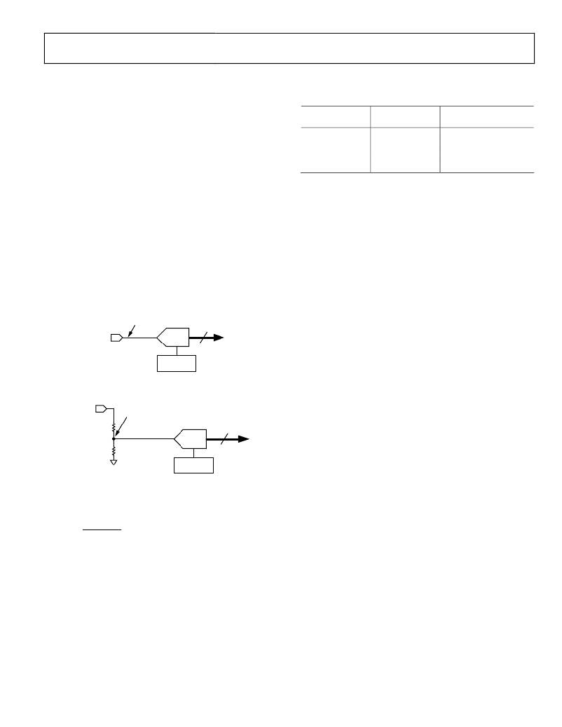
�VXx�
�NO� ATTENUATION�
�12-BIT�
�ADC�
�DIGITIZED�
�VOLTAGE�
�READING�
�the� VX1� pin� can� be� correctly� read� out� as� an� ADC� code� of� approxi-�
�mately� 3/4� full� scale,� but� it� always� sits� above� any� supervisory� limits�
�that� can� be� set� on� that� pin.� The� maximum� setting� for� the� REFIN�
�pin� is� 2.048� V.�
�2.048V� VREF�
�Figure� 30.� ADC� Reading� on� VXx� Pins�
�SUPPLY� SUPERVISION� WITH� THE� ADC�
�In� addition� to� the� readback� capability,� another� level� of� supervision�
�is� provided� by� the� on-chip� 12-bit� ADC.� The� ADM1066� has� limit�
�VPx/VH�
�ATTENUATION� NETWORK�
�(DEPENDS� ON� RANGE� SELECTED)�
�12-BIT�
�ADC�
�DIGITIZED�
�VOLTAGE�
�READING�
�registers� with� which� the� user� can� program� a� maximum� or�
�minimum� allowable� threshold.� Exceeding� the� threshold� generates�
�a� warning� that� can� either� be� read� back� from� the� status� registers�
�or� input� into� the� SE� to� determine� what� sequencing� action� the�
�ADM1066� should� take.� Only� one� register� is� provided� for� each�
�2.048V� VREF�
�Figure� 31.� ADC� Reading� on� VPx/VH� Pins�
�The� voltage� at� the� input� pin� can� be� derived� from� the� following�
�equation:�
�input� channel.� Therefore,� either� an� undervoltage� threshold� or�
�overvoltage� threshold� (but� not� both)� can� be� set� for� a� given� channel.�
�The� round-robin� circuit� can� be� enabled� via� an� SMBus� write,� or�
�it� can� be� programmed� to� turn� on� in� any� state� in� the� SE� program.�
�For� example,� it� can� be� set� to� start� after� a� power-up� sequence� is�
�complete� and� all� supplies� are� known� to� be� within� expected�
�V� =�
�ADC Code�
�4095�
�� Attenuation� Factor� � V� REFIN�
�tolerance� limits.�
�Note� that� a� latency� is� built� into� this� supervision,� dictated� by� the�
�where� V� REFIN� =� 2.048� V� when� the� internal� reference� is� used� (that�
�is,� the� REFIN� pin� is� connected� to� the� REFOUT� pin).�
�The� ADC� input� voltage� ranges� for� the� SFD� input� ranges� are�
��conversion� time� of� the� ADC.� With� all� 12� channels� selected,� the�
�total� time� for� the� round-robin� operation� (averaging� off)� is�
�approximately� 6� ms� (500� μs� per� channel� selected).� Supervision�
�using� the� ADC,� therefore,� does� not� provide� the� same� real-time�
�response� as� the� SFDs.�
�Rev.� E� |� Page� 21� of� 32�
�相关PDF资料 |
PDF描述 |
|---|---|
| LTC3778EF | IC REG CTRLR BUCK PWM CM 20TSSOP |
| ADM1066ACPZ-REEL | IC SEQUENCER/SUPERVISOR 40LFCSP |
| LTC3861EUHE#TRPBF | IC REG CTRLR BUCK PWM VM 36-QFN |
| LT3759HMSE#TRPBF | IC REG CTRLR BST INV PWM 12-MSOP |
| GBC55DCST-S288 | CONN EDGECARD 110POS .100 EXTEND |
相关代理商/技术参数 |
参数描述 |
|---|---|
| ADM1066ASUZ-REEL7 | 功能描述:IC SEQUENCER/SUPERVISOR 48TQFP RoHS:是 类别:集成电路 (IC) >> PMIC - 监控器 系列:Super Sequencer® 标准包装:1 系列:- 类型:简单复位/加电复位 监视电压数目:1 输出:开路漏极或开路集电极 复位:高有效 复位超时:- 电压 - 阀值:1.8V 工作温度:-40°C ~ 125°C 安装类型:表面贴装 封装/外壳:6-TSOP(0.059",1.50mm 宽)5 引线 供应商设备封装:5-TSOP 包装:剪切带 (CT) 其它名称:NCP301HSN18T1GOSCT |
| ADM1067 | 制造商:AD 制造商全称:Analog Devices 功能描述:Super Sequencer with Open-Loop Margining DACs |
| ADM1067ACP | 制造商:Analog Devices 功能描述:Sequencer 40-Pin LFCSP EP |
| ADM1067ACP-REEL | 制造商:Analog Devices 功能描述:Sequencer 40-Pin LFCSP EP T/R |
| ADM1067ACP-REEL7 | 制造商:Analog Devices 功能描述:Sequencer 40-Pin LFCSP EP T/R |
发布紧急采购,3分钟左右您将得到回复。