- 您现在的位置:买卖IC网 > PDF目录15308 > ADM1066ASUZ-REEL (Analog Devices Inc)IC SEQUENCER/SUPERVISOR 48TQFP PDF资料下载
参数资料
| 型号: | ADM1066ASUZ-REEL |
| 厂商: | Analog Devices Inc |
| 文件页数: | 28/32页 |
| 文件大小: | 0K |
| 描述: | IC SEQUENCER/SUPERVISOR 48TQFP |
| 标准包装: | 2,000 |
| 系列: | Super Sequencer® |
| 类型: | 序列发生器 |
| 监视电压数目: | 12 |
| 输出: | 可编程 |
| 电压 - 阀值: | 可调节/可选择 |
| 工作温度: | -40°C ~ 85°C |
| 安装类型: | 表面贴装 |
| 封装/外壳: | 48-TQFP |
| 供应商设备封装: | 48-TQFP(7x7) |
| 包装: | 带卷 (TR) |
| 配用: | EVAL-ADM1066TQEBZ-ND - BOARD EVALUATION FOR ADM1066TQ |
第1页第2页第3页第4页第5页第6页第7页第8页第9页第10页第11页第12页第13页第14页第15页第16页第17页第18页第19页第20页第21页第22页第23页第24页第25页第26页第27页当前第28页第29页第30页第31页第32页
�� �
�
�ADM1066�
�1�
�9�
�1�
�9�
�SCL�
�SDA�
�0�
�1�
�1�
�0�
�1�
�A1�
�A0� R/W�
�D7�
�D6�
�D5�
�D4�
�D3�
�D2�
�D1�
�D0�
�START� BY�
�MASTER�
�ACK.� BY�
�SLAVE�
�ACK.� BY�
�MASTER�
�SCL�
�(CONTINUED)�
�1�
�FRAME� 1�
�SLAVE� ADDRESS�
�9�
�1�
�FRAME� 2�
�DATA� BYTE�
�9�
�SDA�
�(CONTINUED)�
�D7�
�D6�
�D5�
�D4� D3� D2�
�FRAME� 3�
�DATA� BYTE�
�D1�
�D0�
�ACK.� BY�
�MASTER�
�D7�
�D6�
�D5�
�D4� D3� D2�
�FRAME� N�
�DATA� BYTE�
�D1�
�D0�
�NO� ACK.�
�STOP�
�BY�
�MASTER�
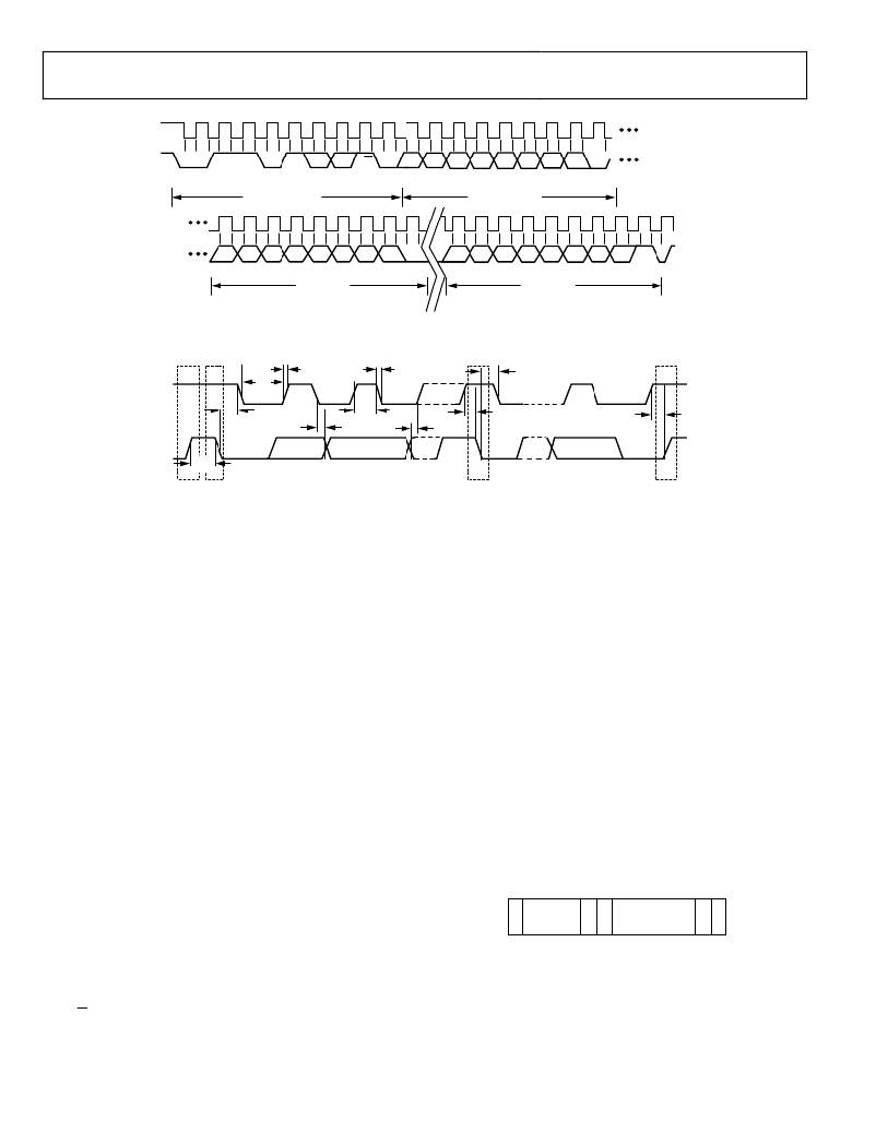
�Figure� 37.� General� SMBus� Read� Timing� Diagram�
�SCL�
�t� LO� W�
�t� R�
�t� F�
�t� HD;� STA�
�t� HD;� STA�
�t� HD;� DAT�
�t� SU;� DAT�
�t� HI� G� H�
�t� SU;� STA�
�t� SU;� STO�
�SDA�
�t� BUF�
�P�
�S�
�S�
�P�
�Figure� 38.� Serial� Bus� Timing� Diagram�
�SLAVE�
�ADDRESS�
�SMBus� PROTOCOLS� FOR� RAM� AND� EEPROM�
�The� ADM1066� contains� volatile� registers� (RAM)� and� nonvolatile�
�registers� (EEPROM).� User� RAM� occupies� Address� 0x00� to�
�Address� 0xDF;� the� EEPROM� occupies� Address� 0xF800� to�
�Address� 0xFBFF.�
�Data� can� be� written� to� and� read� from� both� the� RAM� and� the�
�EEPROM� as� single� data� bytes.� Data� can� be� written� only� to�
�unprogrammed� EEPROM� locations.� To� write� new� data� to� a�
�programmed� location,� the� location� contents� must� first� be� erased.�
�EEPROM� erasure� cannot� be� done� at� the� byte� level.� The� EEPROM�
�is� arranged� as� 32� pages� of� 32� bytes� each,� and� an� entire� page�
�must� be� erased.�
�Page� erasure� is� enabled� by� setting� Bit� 2� in� the� UPDCFG� register�
�(Address� 0x90)� to� 1.� If� this� bit� is� not� set,� page� erasure� cannot�
�occur,� even� if� the� command� byte� (0xFE)� is� programmed� across�
�the� SMBus.�
�WRITE� OPERATIONS�
�The� SMBus� specification� defines� several� protocols� for� different�
�types� of� read� and� write� operations.� The� following� abbreviations�
��?� S� =� Start�
�The� ADM1066� uses� the� following� SMBus� write� protocols.�
�Send� Byte�
�In� a� send� byte� operation,� the� master� device� sends� a� single�
�command� byte� to� a� slave� device,� as� follows:�
�1.� The� master� device� asserts� a� start� condition� on� SDA.�
�2.� The� master� sends� the� 7-bit� slave� address� followed� by� the�
�write� bit� (low).�
�3.� The� addressed� slave� device� asserts� an� acknowledge� (ACK)�
�on� SDA.�
�4.� The� master� sends� a� command� code.�
�5.� The� slave� asserts� an� ACK� on� SDA.�
�6.� The� master� asserts� a� stop� condition� on� SDA,� and� the�
�transaction� ends.�
�In� the� ADM1066,� the� send� byte� protocol� is� used� for� two�
�purposes:�
�?� To� write� a� register� address� to� the� RAM� for� a� subsequent�
�single� byte� read� from� the� same� address,� or� for� a� block� read�
��1� 2� 3� 4� 5� 6�
�RAM�
�S� W� A� ADDRESS� A� P�
�(0x00� TO� 0xDF)�
�?�
�?�
�?�
�?�
�?�
�P� =� Stop�
�R� =� Read�
�W� =� Write�
�A� =� Acknowledge�
�A� =� No� acknowledge�
�?�
�Figure� 39.� Setting� a� RAM� Address� for� Subsequent� Read�
�To� erase� a� page� of� EEPROM� memory.� EEPROM� memory�
�can� be� written� to� only� if� it� is� unprogrammed.� Before� writing�
�to� one� or� more� EEPROM� memory� locations� that� are� already�
�programmed,� the� page(s)� containing� those� locations� must�
�first� be� erased.� EEPROM� memory� is� erased� by� writing� a�
�command� byte.�
�Rev.� E� |� Page� 28� of� 32�
�相关PDF资料 |
PDF描述 |
|---|---|
| LTC3778EF | IC REG CTRLR BUCK PWM CM 20TSSOP |
| ADM1066ACPZ-REEL | IC SEQUENCER/SUPERVISOR 40LFCSP |
| LTC3861EUHE#TRPBF | IC REG CTRLR BUCK PWM VM 36-QFN |
| LT3759HMSE#TRPBF | IC REG CTRLR BST INV PWM 12-MSOP |
| GBC55DCST-S288 | CONN EDGECARD 110POS .100 EXTEND |
相关代理商/技术参数 |
参数描述 |
|---|---|
| ADM1066ASUZ-REEL7 | 功能描述:IC SEQUENCER/SUPERVISOR 48TQFP RoHS:是 类别:集成电路 (IC) >> PMIC - 监控器 系列:Super Sequencer® 标准包装:1 系列:- 类型:简单复位/加电复位 监视电压数目:1 输出:开路漏极或开路集电极 复位:高有效 复位超时:- 电压 - 阀值:1.8V 工作温度:-40°C ~ 125°C 安装类型:表面贴装 封装/外壳:6-TSOP(0.059",1.50mm 宽)5 引线 供应商设备封装:5-TSOP 包装:剪切带 (CT) 其它名称:NCP301HSN18T1GOSCT |
| ADM1067 | 制造商:AD 制造商全称:Analog Devices 功能描述:Super Sequencer with Open-Loop Margining DACs |
| ADM1067ACP | 制造商:Analog Devices 功能描述:Sequencer 40-Pin LFCSP EP |
| ADM1067ACP-REEL | 制造商:Analog Devices 功能描述:Sequencer 40-Pin LFCSP EP T/R |
| ADM1067ACP-REEL7 | 制造商:Analog Devices 功能描述:Sequencer 40-Pin LFCSP EP T/R |
发布紧急采购,3分钟左右您将得到回复。