- 您现在的位置:买卖IC网 > PDF目录15308 > ADM1066ASUZ-REEL (Analog Devices Inc)IC SEQUENCER/SUPERVISOR 48TQFP PDF资料下载
参数资料
| 型号: | ADM1066ASUZ-REEL |
| 厂商: | Analog Devices Inc |
| 文件页数: | 29/32页 |
| 文件大小: | 0K |
| 描述: | IC SEQUENCER/SUPERVISOR 48TQFP |
| 标准包装: | 2,000 |
| 系列: | Super Sequencer® |
| 类型: | 序列发生器 |
| 监视电压数目: | 12 |
| 输出: | 可编程 |
| 电压 - 阀值: | 可调节/可选择 |
| 工作温度: | -40°C ~ 85°C |
| 安装类型: | 表面贴装 |
| 封装/外壳: | 48-TQFP |
| 供应商设备封装: | 48-TQFP(7x7) |
| 包装: | 带卷 (TR) |
| 配用: | EVAL-ADM1066TQEBZ-ND - BOARD EVALUATION FOR ADM1066TQ |
第1页第2页第3页第4页第5页第6页第7页第8页第9页第10页第11页第12页第13页第14页第15页第16页第17页第18页第19页第20页第21页第22页第23页第24页第25页第26页第27页第28页当前第29页第30页第31页第32页
�� �
�
�ADM1066�
�The� master� sends� a� command� code� telling� the� slave� device�
�to� erase� the� page.� The� ADM1066� command� code� for� a� page�
�erasure� is� 0xFE� (1111� 1110).� Note� that� for� a� page� erasure� to�
�1�
�S�
�2�
�SLAVE�
�ADDRESS�
�3�
�W� A�
�4�
�EEPROM�
�ADDRESS�
�HIGH� BYTE�
�(0xF8� TO� 0xFB)�
�5�
�A�
�6�
�EEPROM�
�ADDRESS�
�LOW� BYTE�
�(0x00� TO� 0xFF)�
�7� 8�
�A� P�
�SLAVE�
�ADDRESS�
�take� place,� the� page� address� must� be� given� in� the� previous�
�write� word� transaction� (see� the� Write� Byte/Word� section).� In�
�addition,� Bit� 2� in� the� UPDCFG� register� (Address� 0x90)�
�must� be� set� to� 1.�
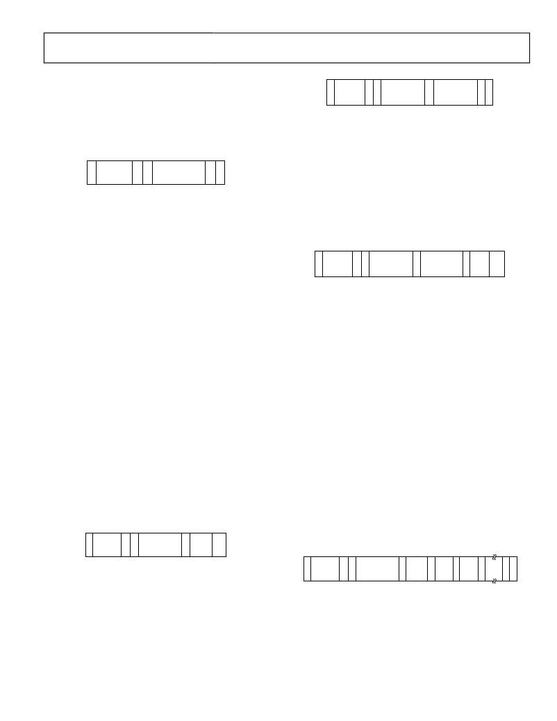
�1� 2� 3� 4� 5� 6�
�COMMAND�
�S� W� A� BYTE� A� P�
�(0xFE)�
�Figure� 42.� Setting� an� EEPROM� Address�
�Because� a� page� consists� of� 32� bytes,� only� the� three� MSBs� of�
�the� address� low� byte� are� important� for� page� erasure.� The�
�lower� five� bits� of� the� EEPROM� address� low� byte� specify� the�
�addresses� within� a� page� and� are� ignored� during� an� erase�
�operation.�
�A�
�A� DATA� A� P�
�S� W� A�
�Figure� 40.� EEPROM� Page� Erasure�
�As� soon� as� the� ADM1066� receives� the� command� byte,�
�page� erasure� begins.� The� master� device� can� send� a� stop�
�command� as� soon� as� it� sends� the� command� byte.� Page�
�erasure� takes� approximately� 20� ms.� If� the� ADM1066� is�
�accessed� before� erasure� is� complete,� it� responds� with� a�
�no� acknowledge� (NACK).�
�Write� Byte/Word�
�?�
�To� write� a� single� byte� of� data� to� the� EEPROM.� In� this� case,�
�the� command� byte� is� the� high� byte� of� EEPROM� Address� 0xF8�
�to� EEPROM� Address� 0xFB.� The� first� data� byte� is� the� low�
�byte� of� the� EEPROM� address,� and� the� second� data� byte� is�
��1� 2� 3� 4� 5� 6� 7� 8� 9� 10�
�EEPROM� EEPROM�
�SLAVE� ADDRESS� ADDRESS�
�ADDRESS� HIGH� BYTE� LOW� BYTE�
�(0xF8� TO� 0xFB)� (0x00� TO� 0xFF)�
�In� a� write� byte/word� operation,� the� master� device� sends� a�
�command� byte� and� one� or� two� data� bytes� to� the� slave� device,� as�
�follows:�
�Figure� 43.� Single� Byte� Write� to� the� EEPROM�
�Block� Write�
�In� a� block� write� operation,� the� master� device� writes� a� block� of�
�1.�
�2.�
�3.�
�The� master� device� asserts� a� start� condition� on� SDA.�
�The� master� sends� the� 7-bit� slave� address� followed� by� the�
�write� bit� (low).�
�The� addressed� slave� device� asserts� an� ACK� on� SDA.�
�data� to� a� slave� device.� The� start� address� for� a� block� write� must�
�have� been� set� previously.� In� the� ADM1066,� a� send� byte� opera-�
�tion� sets� a� RAM� address,� and� a� write� byte/word� operation� sets�
�an� EEPROM� address,� as� follows:�
�4.�
�5.�
�6.�
�7.�
�8.�
�9.�
�The� master� sends� a� command� code.�
�The� slave� asserts� an� ACK� on� SDA.�
�The� master� sends� a� data� byte.�
�The� slave� asserts� an� ACK� on� SDA.�
�The� master� sends� a� data� byte� or� asserts� a� stop� condition.�
�The� slave� asserts� an� ACK� on� SDA.�
�1.�
�2.�
�3.�
�4.�
�The� master� device� asserts� a� start� condition� on� SDA.�
�The� master� sends� the� 7-bit� slave� address� followed� by�
�the� write� bit� (low).�
�The� addressed� slave� device� asserts� an� ACK� on� SDA.�
�The� master� sends� a� command� code� that� tells� the� slave�
�device� to� expect� a� block� write.� The� ADM1066� command�
�10.� The� master� asserts� a� stop� condition� on� SDA� to� end� the�
�code� for� a� block� write� is� 0xFC� (1111� 1100).�
�transaction.�
�In� the� ADM1066,� the� write� byte/word� protocol� is� used� for� three�
�purposes:�
�?� To� write� a� single� byte� of� data� to� the� RAM.� In� this� case,� the�
�command� byte� is� RAM� Address� 0x00� to� RAM� Address� 0xDF,�
��5.�
�6.�
�7.�
�8.�
�9.�
�The� slave� asserts� an� ACK� on� SDA.�
�The� master� sends� a� data� byte� that� tells� the� slave� device� how�
�many� data� bytes� are� being� sent.� The� SMBus� specification�
�allows� a� maximum� of� 32� data� bytes� in� a� block� write.�
�The� slave� asserts� an� ACK� on� SDA.�
�The� master� sends� N� data� bytes.�
�The� slave� asserts� an� ACK� on� SDA� after� each� data� byte.�
�1�
�2�
�3�
�4�
�5�
�6�
�7� 8�
�10.� The� master� asserts� a� stop� condition� on� SDA� to� end� the�
�S� ADDRESS� W� A�
�SLAVE�
�RAM�
�ADDRESS�
�(0x00� TO� 0xDF)�
�A� DATA� A� P�
�1�
�transaction.�
�2� 3�
�4�
�5�
�6�
�7�
�8�
�9�
�10�
�W� A� COMMAND� 0xFC� A�
�A� DATA� A� DATA� A� DATA� A� P�
�?�
�Figure� 41.� Single� Byte� Write� to� the� RAM�
�To� set� up� a� 2-byte� EEPROM� address� for� a� subsequent� read,�
�S�
�SLAVE�
�ADDRESS�
�(BLOCK� WRITE)�
�BYTE�
�COUNT�
�1� 2� N�
�write,� block� read,� block� write,� or� page� erase.� In� this� case,� the�
�command� byte� is� the� high� byte� of� EEPROM� Address� 0xF8�
�to� EEPROM� Address� 0xFB.� The� only� data� byte� is� the� low�
��Rev.� E� |� Page� 29� of� 32�
�Figure� 44.� Block� Write� to� the� EEPROM� or� RAM�
�相关PDF资料 |
PDF描述 |
|---|---|
| LTC3778EF | IC REG CTRLR BUCK PWM CM 20TSSOP |
| ADM1066ACPZ-REEL | IC SEQUENCER/SUPERVISOR 40LFCSP |
| LTC3861EUHE#TRPBF | IC REG CTRLR BUCK PWM VM 36-QFN |
| LT3759HMSE#TRPBF | IC REG CTRLR BST INV PWM 12-MSOP |
| GBC55DCST-S288 | CONN EDGECARD 110POS .100 EXTEND |
相关代理商/技术参数 |
参数描述 |
|---|---|
| ADM1066ASUZ-REEL7 | 功能描述:IC SEQUENCER/SUPERVISOR 48TQFP RoHS:是 类别:集成电路 (IC) >> PMIC - 监控器 系列:Super Sequencer® 标准包装:1 系列:- 类型:简单复位/加电复位 监视电压数目:1 输出:开路漏极或开路集电极 复位:高有效 复位超时:- 电压 - 阀值:1.8V 工作温度:-40°C ~ 125°C 安装类型:表面贴装 封装/外壳:6-TSOP(0.059",1.50mm 宽)5 引线 供应商设备封装:5-TSOP 包装:剪切带 (CT) 其它名称:NCP301HSN18T1GOSCT |
| ADM1067 | 制造商:AD 制造商全称:Analog Devices 功能描述:Super Sequencer with Open-Loop Margining DACs |
| ADM1067ACP | 制造商:Analog Devices 功能描述:Sequencer 40-Pin LFCSP EP |
| ADM1067ACP-REEL | 制造商:Analog Devices 功能描述:Sequencer 40-Pin LFCSP EP T/R |
| ADM1067ACP-REEL7 | 制造商:Analog Devices 功能描述:Sequencer 40-Pin LFCSP EP T/R |
发布紧急采购,3分钟左右您将得到回复。