- 您现在的位置:买卖IC网 > PDF目录375258 > ADM1192-1ARMZ-R7 (ANALOG DEVICES INC) Digital Power Monitor with Clear Pin and ALERT Output PDF资料下载
参数资料
| 型号: | ADM1192-1ARMZ-R7 |
| 厂商: | ANALOG DEVICES INC |
| 元件分类: | 电源管理 |
| 英文描述: | Digital Power Monitor with Clear Pin and ALERT Output |
| 中文描述: | 1-CHANNEL POWER SUPPLY MANAGEMENT CKT, PDSO10 |
| 封装: | LEAD FREE, MO-187BA, MSOP-10 |
| 文件页数: | 15/20页 |
| 文件大小: | 274K |
| 代理商: | ADM1192-1ARMZ-R7 |
ADM1192
Table 15. Status Byte Operations
Bit
Name
0
ADC_OC
1
ADC_ALERT
Rev. 0 | Page 15 of 20
Function
An ADC-based overcurrent comparison has been detected on the last three conversions.
An ADC-based overcurrent trip has occurred, which has caused the alert. Cleared by writing to Bit 4 of the ALERT_EN
register.
An overcurrent condition is present (that is, the output of the current sense amplifier is greater than the voltage on the
SETV input).
An overcurrent condition has caused the ALERT block to latch a fault, and the ALERT output has asserted. Cleared by
writing to Bit 4 of the ALERT_EN register.
Set to 1 by writing to the SWOFF bit of the CONTROL register.
An alert has been caused by the SWOFF bit. Cleared by writing to Bit 4 of the ALERT_EN register.
2
OC
3
OC_ALERT
4
5
ALERT OUTPUT
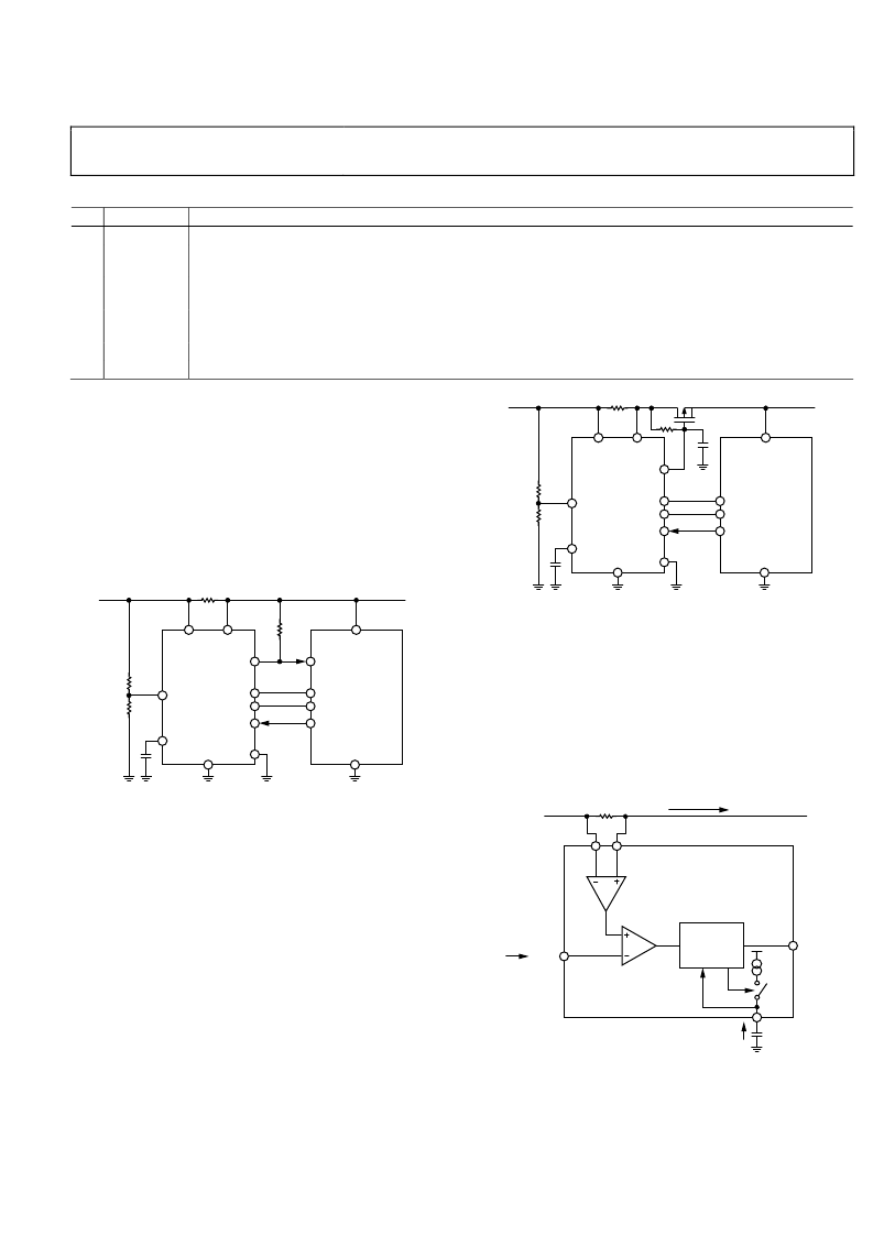
The ALERT output is an open-drain pin with 30 V tolerance.
There are two uses for this output.
OFF_STATUS
OFF_ALERT
Overcurrent Flag
The ALERT pin can be connected to the general-purpose logic
input of a controller. Under normal operation, the ADM1192
drives this output low. When an overcurrent condition occurs,
the output asserts high. An external pull-up resistor should
be used.
R
SENSE
P = VI
CONTROLLER
ADM1192
SENSE
VCC
SDA
SCL
SDA
SCL
GND
ALERT
CLRB
CLRB
ADR
TIMER
3.15V TO 26V
SETV
ALERT
0
Figure 27. Using the ALERT Output as an Interrupt
Implementing a Basic Hot Swap Circuit
A basic P-channel FET hot swap circuit can be created. The
ALERT output should be connected to the GATE pin of a
P-channel FET connected in series with the power path. A pull-
up from GATE to source ensures that the P-channel FET GATE
is pulled up and the device held off as soon as power is applied.
When the ADM1192 powers up, the GATE is pulled low by the
ALERT output. A capacitor on the TIMER pin determines the
slew rate of the GATE at turn-on. Note that if a current fault
occurs at any point in operation, the ALERT output asserts
high, turning off the P-channel FET.
R
SENSE
P-CHANNEL FET
P = VI
CONTROLLER
ADM1192
SENSE
VCC
SDA
SCL
SDA
SCL
GND
ALERT
CLRB
CLRB
ADR
TIMER
3.15V TO 26V
SETV
0
Figure 28. P-Channel FET Hot Swap Implementation
SETV PIN
The SETV pin allows the user to adjust the current level that
trips the ALERT output. The output of the current sense amplifier
is compared with the voltage driven onto the SETV pin. If the
current sense amplifier output is higher than the SETV voltage,
the output of the comparator asserts. By driving a different voltage
onto the SETV pin, the ADM1192 detects an overcurrent condition
at a different current level, with a gain of 18. See Figure 12 for
an illustration of this relationship.
ADM1192
SETV
1.3V
ALERT
CURRENT
SENSE
AMPLIFIER
A
ALERT
60μA
R
SENSE
I
LOAD
APPLIED
VOLTAGE
SENSE
VCC
TIMER
COMPARATOR
0
Figure 29. SETV Operation
相关PDF资料 |
PDF描述 |
|---|---|
| ADM14185E | RS-232 Line Drivers/Receivers(±15kV ESD保护,RS-232线驱动器/接收器) |
| ADM14196E | RS-232 Line Drivers/Receivers(±15kV ESD保护,RS-232线驱动器/接收器) |
| ADM208E | RS-232 Line Drivers/Receivers(15kV ESD保护,RS-232线驱动器/接收器) |
| ADM209 | +5 V Powered CMOS RS-232 Drivers/Receivers(CMOS RS-232驱动器/接收器) |
| ADM213 | +5 V Powered CMOS RS-232 Drivers/Receivers(CMOS RS-232驱动器/接收器) |
相关代理商/技术参数 |
参数描述 |
|---|---|
| ADM1192ARMZ-R7 | 功能描述:IC PWR MONITOR DGTL ALERT 10MSOP RoHS:是 类别:集成电路 (IC) >> PMIC - 电源管理 - 专用 系列:- 应用说明:Ultrasound Imaging Systems Application Note 产品培训模块:Lead (SnPb) Finish for COTS Obsolescence Mitigation Program 标准包装:37 系列:- 应用:医疗用超声波成像,声纳 电流 - 电源:- 电源电压:2.37 V ~ 6 V 工作温度:0°C ~ 70°C 安装类型:表面贴装 封装/外壳:56-WFQFN 裸露焊盘 供应商设备封装:56-TQFN-EP(8x8) 包装:管件 |
| ADM1232 | 制造商:AD 制造商全称:Analog Devices 功能描述:Microprocessor Supervisory Circuit |
| ADM1232_08 | 制造商:AD 制造商全称:Analog Devices 功能描述:Microprocessor Supervisory Circuit |
| ADM1232A | 制造商:AD 制造商全称:Analog Devices 功能描述:Microprocessor Supervisory Circuit |
| ADM1232AAN | 制造商:AD 制造商全称:Analog Devices 功能描述:Microprocessor Supervisory Circuit |
发布紧急采购,3分钟左右您将得到回复。