- 您现在的位置:买卖IC网 > PDF目录15323 > ADM8690ANZ (Analog Devices Inc)IC SUPERVISOR MPU 4.65V 8DIP PDF资料下载
参数资料
| 型号: | ADM8690ANZ |
| 厂商: | Analog Devices Inc |
| 文件页数: | 11/24页 |
| 文件大小: | 0K |
| 描述: | IC SUPERVISOR MPU 4.65V 8DIP |
| 标准包装: | 50 |
| 类型: | 备用电池电路 |
| 监视电压数目: | 1 |
| 输出: | 推挽式,图腾柱 |
| 复位: | 低有效 |
| 复位超时: | 最小为 35 ms |
| 电压 - 阀值: | 4.65V |
| 工作温度: | -40°C ~ 85°C |
| 安装类型: | 通孔 |
| 封装/外壳: | 8-DIP(0.300",7.62mm) |
| 供应商设备封装: | 8-PDIP |
| 包装: | 管件 |
�� ��
��
��Data� Sheet�
�CIRCUIT� INFORMATION�
�BATTERY� SWITCHOVER� SECTION�
�The� battery� switchover� circuit� compares� V� CC� to� the� V� BATT�
�input� and� connects� V� OUT� to� whichever� is� higher.� Switchover�
�occurs� when� V� CC� is� 50� mV� higher� than� V� BATT� as� V� CC� falls,� and�
�when� V� CC� is� 70� mV� greater� than� V� BATT� as� V� CC� rises.� This� 20� mV�
�hysteresis� prevents� repeated� rapid� switching� if� V� CC� falls� very�
�slowly� or� remains� nearly� equal� to� the� battery� voltage.�
�ADM8690/ADM8691/ADM8695�
�If� the� battery� switchover� section� is� not� used,� V� BATT� should� be�
�connected� to� GND� and� V� OUT� should� be� connected� to� V� CC� .�
�POWER-FAIL� RESET� OUTPUT�
�RESET� is� an� active� low� output� that� provides� a� RESET� signal� to�
�the� microprocessor� whenever� V� CC� is� at� an� invalid� level.� When�
�V� CC� falls� below� the� reset� threshold,� the� RESET� output� is� forced�
�low.� The� nominal� reset� voltage� threshold� is� 4.65� V.�
�V� CC�
�V� OUT�
�V� CC�
�V2�
�V1�
�V2�
�V1�
�V� BATT�
�GATE� DRIVE�
�100�
�mV�
�INTERNAL�
�SHUTDOWN� SIGNAL�
�BATT� ON�
�(ADM8691,�
�ADM8695)�
�RESET�
�LOW� LINE�
�t� 1�
�t� 1�
�700�
�mV�
�WHEN�
�V� BATT� >� (V� CC� +� 0.7V)�
�t1� =� RESET� TIME�
�V1� =� RESET� VOLTAGE� THRESHOLD� LOW�
�V2� =� RESET� VOLTAGE� THRESHOLD� HIGH�
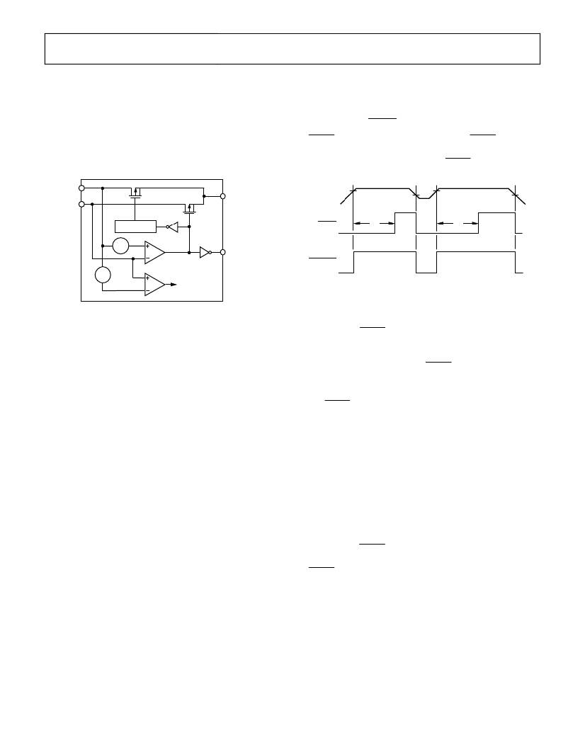
�Figure� 14.� Battery� Switchover� Schematic�
�During� normal� operation,� with� V� CC� higher� than� V� BATT� ,� V� CC�
�is� internally� switched� to� V� OUT� through� an� internal� PMOS� tran-�
�sistor� switch.� This� switch� has� a� typical� on� resistance� of� 0.7� Ω�
�and� can� supply� up� to� 100� mA� at� the� V� OUT� terminal.� V� OUT� is�
�normally� used� to� drive� a� RAM� memory� bank,� requiring�
�instantaneous� currents� of� greater� than� 100� mA.� If� this� is� the�
�case,� a� bypass� capacitor� should� be� connected� to� V� OUT� .� The�
�capacitor� provides� the� peak� current� transients� to� the� RAM.�
�A� capacitance� value� of� 0.1� μF� or� greater� can� be� used.�
�If� the� continuous� output� current� requirements� at� V� OUT� exceed�
�100� mA� or� if� a� lower� V� CC� ?� V� OUT� voltage� differential� is� desired,�
�an� external� PNP� pass� transistor� can� be� connected� in� parallel�
���(see� Figure� 24).�
�A� 7� Ω� MOSFET� switch� connects� the� V� BATT� input� to� V� OUT� during�
�battery� backup.� This� MOSFET� has� very� low� input-to-output�
�differential� (dropout� voltage)� at� the� low� current� levels� required�
�for� battery� backup� of� CMOS� RAM� or� other� low� power� CMOS�
�circuitry.� The� supply� current� in� battery� backup� is� typically� 0.4� μA.�
�The� ADM8690� /� ADM8691� /� ADM8695� operate� with� battery�
�voltages� from� 2.0� V� to� 4.25� V.� High� value� capacitors,� either� standard�
�electrolytic� or� the� farad-size,� double-layer� capacitors,� can� also� be�
�HYSTERESIS� =� V2� –� V1�
�Figure� 15.� Power-Fail� Reset� Timing�
�On� power-up,� RESET� remains� low� for� 50� ms� (200� ms� for� the�
��old.� This� allows� time� for� the� power� supply� and� microprocessor�
�to� stabilize.� On� power-down,� the� RESET� output� remains� low�
�with� V� CC� as� low� as� 1� V.� This� ensures� that� the� microprocessor� is�
�held� in� a� stable� shutdown� condition.�
��ADM8695� by� using� an� external� oscillator� or� by� connecting� an�
���The� guaranteed� minimum� and� maximum� reset� thresholds� for�
�the� ADM8690� /� ADM8691� /� ADM8695� are� 4.5� V� and� 4.73� V.� The�
��5� V� supplies� with� a� +10%,� ?5%� tolerance.� The� reset� threshold�
�comparator� typically� has� 40� mV� of� hysteresis.� The� response� time�
�of� the� reset� voltage� comparator� is� less� than� 1� μs.� If� glitches� are�
�present� on� the� V� CC� line� that� could� cause� spurious� reset� pulses,�
�V� CC� should� be� decoupled� close� to� the� device.�
�In� addition� to� RESET,� the� ADM8691� /� ADM8695� provide� an�
�active� high� RESET� output.� This� output� is� the� complement� of�
�RESET� and� is� intended� for� processors� that� require� an� active�
�high� reset� signal.�
�used� for� short-term� memory� backup.� A� small� charging� current�
�of� typically� 10� nA� (0.1� μA� maximum)� flows� out� of� the� V� BATT�
�terminal.� This� current� is� useful� for� maintaining� rechargeable�
�batteries� in� a� fully� charged� condition.� This� extends� the� life� of� the�
�backup� battery� by� compensating� for� its� self-discharge� current.�
�Also� note� that� this� current� poses� no� problem� when� lithium�
�batteries� are� used� for� backup� because� the� maximum� charging�
�current� (0.1� μA)� is� safe� for� even� the� smallest� lithium� cells.�
�Rev.� C� |� Page� 11� of� 24�
�相关PDF资料 |
PDF描述 |
|---|---|
| ELJ-RE1N5ZF2 | INDUCTOR 1.5NH +-.2NH FIXED SMD |
| ELJ-RER10GF3 | INDUCTOR 100NH 2% FIXED SMD |
| ELJ-RE56NGF3 | INDUCTOR 56NH 2% FIXED SMD |
| VE-2WJ-EW-F4 | CONVERTER MOD DC/DC 36V 100W |
| ELJ-RE47NGF2 | INDUCTOR 47NH 2% FIXED SMD |
相关代理商/技术参数 |
参数描述 |
|---|---|
| ADM8690ARN | 功能描述:IC SUPERVISOR MPU 4.65V 8SOIC RoHS:否 类别:集成电路 (IC) >> PMIC - 监控器 系列:- 标准包装:1 系列:- 类型:简单复位/加电复位 监视电压数目:1 输出:开路漏极或开路集电极 复位:高有效 复位超时:- 电压 - 阀值:1.8V 工作温度:-40°C ~ 125°C 安装类型:表面贴装 封装/外壳:6-TSOP(0.059",1.50mm 宽)5 引线 供应商设备封装:5-TSOP 包装:剪切带 (CT) 其它名称:NCP301HSN18T1GOSCT |
| ADM8690ARN-REEL | 功能描述:IC SUPERVISOR MPU 4.65V 8SOIC TR RoHS:否 类别:集成电路 (IC) >> PMIC - 监控器 系列:- 标准包装:1 系列:- 类型:简单复位/加电复位 监视电压数目:1 输出:开路漏极或开路集电极 复位:高有效 复位超时:- 电压 - 阀值:1.8V 工作温度:-40°C ~ 125°C 安装类型:表面贴装 封装/外壳:6-TSOP(0.059",1.50mm 宽)5 引线 供应商设备封装:5-TSOP 包装:剪切带 (CT) 其它名称:NCP301HSN18T1GOSCT |
| ADM8690ARNZ | 功能描述:IC SUPERVISOR MPU 4.65V 8SOIC RoHS:是 类别:集成电路 (IC) >> PMIC - 监控器 系列:- 其它有关文件:STM6717 View All Specifications 标准包装:1 系列:- 类型:多压监控器 监视电压数目:2 输出:开路漏极或开路集电极 复位:低有效 复位超时:最小为 600 ms 电压 - 阀值:1.11V,3.075V 工作温度:-40°C ~ 85°C 安装类型:表面贴装 封装/外壳:SC-74A,SOT-753 供应商设备封装:SOT-23-5 包装:Digi-Reel® 产品目录页面:1194 (CN2011-ZH PDF) 其它名称:497-7019-6 |
| ADM8691 | 制造商:AD 制造商全称:Analog Devices 功能描述:Microprocessor Supervisory Circuits |
| ADM8691AN | 制造商:Analog Devices 功能描述:Processor Supervisor 4.65V 4.75V to 5.5V 16-Pin PDIP 制造商:Rochester Electronics LLC 功能描述:IMPROVED ADM691 I.C. - Bulk 制造商:Analog Devices 功能描述:IC SUPERVISORY CCT 8691 DIP16 |
发布紧急采购,3分钟左右您将得到回复。