- 您现在的位置:买卖IC网 > PDF目录15323 > ADM8690ANZ (Analog Devices Inc)IC SUPERVISOR MPU 4.65V 8DIP PDF资料下载
参数资料
| 型号: | ADM8690ANZ |
| 厂商: | Analog Devices Inc |
| 文件页数: | 7/24页 |
| 文件大小: | 0K |
| 描述: | IC SUPERVISOR MPU 4.65V 8DIP |
| 标准包装: | 50 |
| 类型: | 备用电池电路 |
| 监视电压数目: | 1 |
| 输出: | 推挽式,图腾柱 |
| 复位: | 低有效 |
| 复位超时: | 最小为 35 ms |
| 电压 - 阀值: | 4.65V |
| 工作温度: | -40°C ~ 85°C |
| 安装类型: | 通孔 |
| 封装/外壳: | 8-DIP(0.300",7.62mm) |
| 供应商设备封装: | 8-PDIP |
| 包装: | 管件 |
�� ��
��
��Data� Sheet�
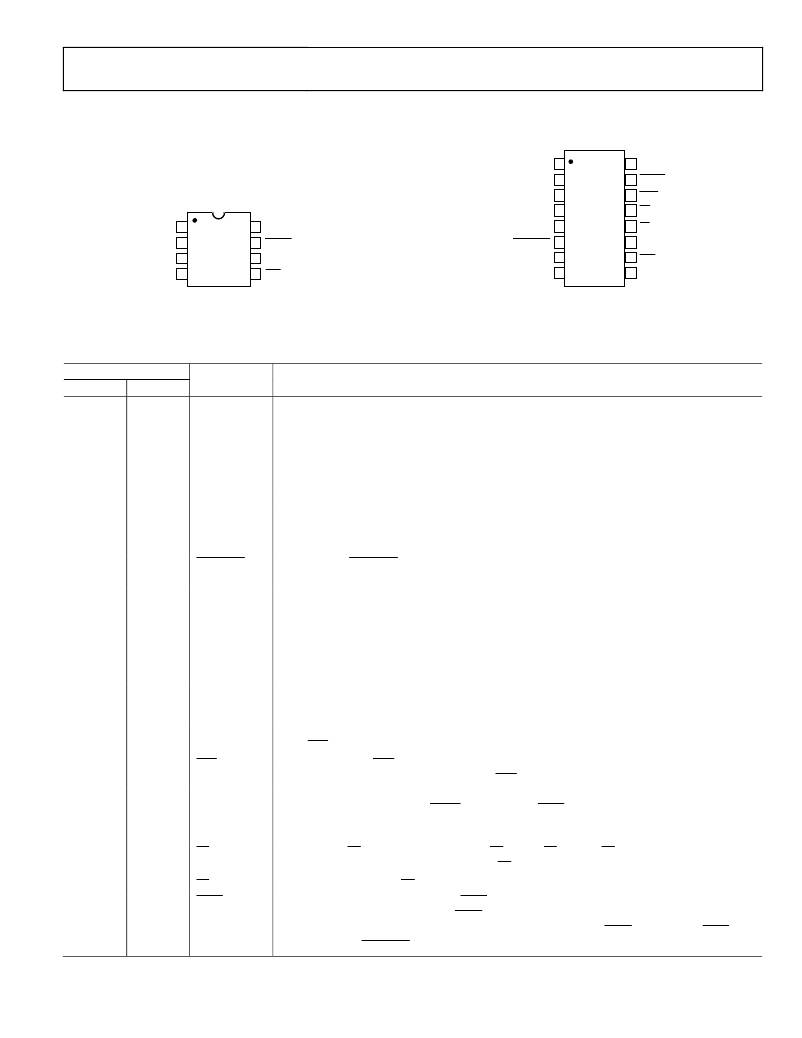
�PIN� CONFIGURATIONS� AND� FUNCTION� DESCRIPTIONS�
�ADM8690/ADM8691/ADM8695�
�V� BATT� 1�
�V� OUT� 2�
�16� RESET�
�15� RESET�
�V� CC� 3�
�GND� 4�
�ADM8691/�
�ADM8695�
�14� WDO�
�13� CE� IN�
�V� OUT� 1�
�V� CC� 2�
�GND� 3�
�PFI� 4�
�ADM8690�
�TOP� VIEW�
�(Not� to� Scale)�
�8� V� BATT�
�7� RESET�
�6� WDI�
�5� PFO�
�BATT� ON� 5�
�LOW� LINE� 6�
�OSC� IN� 7�
�OSC� SEL� 8�
�TOP� VIEW�
�(Not� to� Scale)�
�12� CE� OUT�
�11� WDI�
�10� PFO�
�9� PFI�
�Figure� 3.� ADM8690� Pin� Configuration,�
�8-Lead� PDIP� and� 8-Lead� SOIC_N�
�Table� 4.� Pin� Function� Descriptions�
�Pin� No.�
�Figure� 4.� ADM8691� /� ADM8695� Pin� Configuration,� 16-Lead� PDIP,�
�16-Lead� SOIC_N,� 16-Lead� SOIC_W,� and� 16-Lead� TSSOP�
�8-Lead�
�8�
�16-Lead�
�1�
�Mnemonic�
�V� BATT�
�Description�
�Backup� Battery� Input.� V� BATT� or� V� CC� is� internally� switched� to� V� OUT� ,� depending� on� which� is� at� the�
�highest� potential.�
�1�
�2�
�V� OUT�
�Output� Voltage.� V� CC� or� V� BATT� is� internally� switched� to� V� OUT� ,� depending� on� which� is� at� the� highest�
�potential.� V� OUT� can� supply� up� to� 100� mA� to� power� CMOS� RAM.� Connect� V� OUT� to� V� CC� if� V� OUT� and� V� BATT�
�are� not� used.�
�2�
�3�
�V� CC�
�Power� Supply� Input.� 5� V� nominal.� V� CC� or� V� BATT� is� internally� switched� to� V� OUT� ,� depending� on� which� is�
�at� the� highest� potential.�
�3�
�N/A�
�4�
�5�
�GND�
�BATT� ON�
�Ground.� This� is� the� 0� V� ground� reference� for� all� signals.�
�Logic� Output.� BATT� ON� goes� high� when� V� OUT� is� internally� switched� to� the� V� BATT� input.� It� goes� low�
�when� V� OUT� is� internally� switched� to� V� CC� .� The� output� typically� sinks� 35� mA� and� can� directly� drive� the�
�base� of� an� external� PNP� transistor� to� increase� the� output� current� above� the� 100� mA� rating� of� V� OUT� .�
�N/A�
�6�
�LOW� LINE�
�Logic� Output.� LOW� LINE� goes� low� when� V� CC� falls� below� the� reset� threshold.� It� returns� high� as�
�soon� as� V� CC� rises� above� the� reset� threshold.�
�N/A�
�7�
�OSC� IN�
�Oscillator� Logic� Input.� When� OSC� SEL� is� low,� OSC� IN� can� be� driven� by� an� external� clock� signal,� or�
�an� external� capacitor� can� be� connected� between� OSC� IN� and� GND.� This� sets� both� the� reset� active�
�pulse� timing� and� the� watchdog� timeout� period� (see� Table� 5� and� Figure� 17� through� Figure� 20).�
�When� OSC� SEL� is� high� or� floating,� the� internal� oscillator� is� enabled� and� the� reset� active� time� is�
�fixed� at� 50� ms� typical� (� ADM8691� )� or� 200� ms� typical� (� ADM8695� ).� In� this� mode,� the� OSC� IN� pin�
�selects� either� the� fast� (100� ms)� or� slow� (1.6� sec)� watchdog� timeout� period.� In� both� modes,� the�
�timeout� period� immediately� after� a� reset� is� 1.6� sec� typical.�
�N/A�
�8�
�OSC� SEL�
�Logic� Oscillator� Select� Input.� When� OSC� SEL� is� unconnected� (floating)� or� driven� high,� the� internal�
�oscillator� sets� the� reset� active� time� and� watchdog� timeout� period.� When� OSC� SEL� is� low,� the�
�external� oscillator� input,� OSC� IN,� is� enabled� (see� Table� 5).� OSC� SEL� has� a� 5� μA� internal� pull-up.�
�4�
�9�
�PFI�
�Power-Fail� Input.� PFI� is� the� noninverting� input� to� the� power-fail� comparator.� When� PFI� is� less� than�
�1.3� V,� PFO� goes� low.� Connect� PFI� to� GND� or� V� OUT� when� not� used.�
�5�
�10�
�PFO�
�Power-Fail� Output.� PFO� is� the� output� of� the� power-fail� comparator.� It� goes� low� when� PFI� is� less�
�than� 1.3� V.� The� comparator� is� turned� off� and� PFO� goes� low� when� V� CC� is� below� V� BATT� .�
�6�
�11�
�WDI�
�Watchdog� Input.� WDI� is� a� three-level� input.� If� WDI� remains� either� high� or� low� for� longer� than�
�the� watchdog� timeout� period,� RESET� pulses� low� and� WDO� goes� low.� The� timer� is� reset� with� each�
�transition� on� the� WDI� line.� The� watchdog� timer� can� be� disabled� if� WDI� is� left� floating� or� is� driven�
�to� midsupply.�
�N/A�
�12�
�CE� OUT�
�Logic� Output.� CE� OUT� is� a� gated� version� of� the� CE� IN� signal.� CE� OUT� tracks� CE� IN� when� V� CC� is� above� the� reset�
�threshold.� If� V� CC� is� below� the� reset� threshold,� CE� OUT� is� forced� high.� See� Figure� 21� and� Figure� 22� .�
�N/A�
�N/A�
�13�
�14�
�CE� IN�
�WDO�
�Logic� Input.� Input� to� the� CE� gating� circuit.� When� not� in� use,� connect� this� pin� to� GND� or� V� OUT� .�
�Logic� Output.� The� watchdog� output,� WDO,� goes� low� if� WDI� remains� either� high� or� low� for� longer�
�than� the� watchdog� timeout� period.� WDO� is� set� high� by� the� next� transition� at� WDI.� If� WDI� is�
�unconnected� or� at� midsupply,� the� watchdog� timer� is� disabled� and� WDO� remains� high.� WDO� also�
�goes� high� when� LOW� LINE� goes� low.�
�Rev.� C� |� Page� 7� of� 24�
�相关PDF资料 |
PDF描述 |
|---|---|
| ELJ-RE1N5ZF2 | INDUCTOR 1.5NH +-.2NH FIXED SMD |
| ELJ-RER10GF3 | INDUCTOR 100NH 2% FIXED SMD |
| ELJ-RE56NGF3 | INDUCTOR 56NH 2% FIXED SMD |
| VE-2WJ-EW-F4 | CONVERTER MOD DC/DC 36V 100W |
| ELJ-RE47NGF2 | INDUCTOR 47NH 2% FIXED SMD |
相关代理商/技术参数 |
参数描述 |
|---|---|
| ADM8690ARN | 功能描述:IC SUPERVISOR MPU 4.65V 8SOIC RoHS:否 类别:集成电路 (IC) >> PMIC - 监控器 系列:- 标准包装:1 系列:- 类型:简单复位/加电复位 监视电压数目:1 输出:开路漏极或开路集电极 复位:高有效 复位超时:- 电压 - 阀值:1.8V 工作温度:-40°C ~ 125°C 安装类型:表面贴装 封装/外壳:6-TSOP(0.059",1.50mm 宽)5 引线 供应商设备封装:5-TSOP 包装:剪切带 (CT) 其它名称:NCP301HSN18T1GOSCT |
| ADM8690ARN-REEL | 功能描述:IC SUPERVISOR MPU 4.65V 8SOIC TR RoHS:否 类别:集成电路 (IC) >> PMIC - 监控器 系列:- 标准包装:1 系列:- 类型:简单复位/加电复位 监视电压数目:1 输出:开路漏极或开路集电极 复位:高有效 复位超时:- 电压 - 阀值:1.8V 工作温度:-40°C ~ 125°C 安装类型:表面贴装 封装/外壳:6-TSOP(0.059",1.50mm 宽)5 引线 供应商设备封装:5-TSOP 包装:剪切带 (CT) 其它名称:NCP301HSN18T1GOSCT |
| ADM8690ARNZ | 功能描述:IC SUPERVISOR MPU 4.65V 8SOIC RoHS:是 类别:集成电路 (IC) >> PMIC - 监控器 系列:- 其它有关文件:STM6717 View All Specifications 标准包装:1 系列:- 类型:多压监控器 监视电压数目:2 输出:开路漏极或开路集电极 复位:低有效 复位超时:最小为 600 ms 电压 - 阀值:1.11V,3.075V 工作温度:-40°C ~ 85°C 安装类型:表面贴装 封装/外壳:SC-74A,SOT-753 供应商设备封装:SOT-23-5 包装:Digi-Reel® 产品目录页面:1194 (CN2011-ZH PDF) 其它名称:497-7019-6 |
| ADM8691 | 制造商:AD 制造商全称:Analog Devices 功能描述:Microprocessor Supervisory Circuits |
| ADM8691AN | 制造商:Analog Devices 功能描述:Processor Supervisor 4.65V 4.75V to 5.5V 16-Pin PDIP 制造商:Rochester Electronics LLC 功能描述:IMPROVED ADM691 I.C. - Bulk 制造商:Analog Devices 功能描述:IC SUPERVISORY CCT 8691 DIP16 |
发布紧急采购,3分钟左右您将得到回复。