参数资料
| 型号: | ADN2807ACPZ |
| 厂商: | Analog Devices Inc |
| 文件页数: | 20/20页 |
| 文件大小: | 0K |
| 描述: | IC CLOCK/DATA RECOVERY 48LFCSP |
| 标准包装: | 1 |
| 类型: | 时钟和数据恢复(CDR),多路复用器 |
| PLL: | 是 |
| 主要目的: | SONET/SDH,STM |
| 输入: | CML |
| 输出: | CML |
| 电路数: | 1 |
| 比率 - 输入:输出: | 1:2 |
| 差分 - 输入:输出: | 是/是 |
| 频率 - 最大: | 622MHz |
| 电源电压: | 3 V ~ 3.6 V |
| 工作温度: | -40°C ~ 85°C |
| 安装类型: | 表面贴装 |
| 封装/外壳: | 48-VFQFN 裸露焊盘,CSP |
| 供应商设备封装: | 48-LFCSP |
| 包装: | 托盘 |
ADN2807
Rev. A | Page 9 of 20
LOS RESPONSE TIME
The LOS response time is the delay between the removal of the
input signal and indication of loss of signal (LOS) at SDOUT.
The ADN2807’s response time is 300 ns typ when the inputs are
dc-coupled. In practice, the time constant of ac coupling at the
quantizer input determines the LOS response time.
JITTER SPECIFICATIONS
The ADN2807 CDR is designed to achieve the best bit-error-
rate (BER) performance, and has exceeded the jitter transfer,
generation, and tolerance specifications proposed for
SONET/SDH equipment defined in the Telcordia Technologies
specification. Jitter is the dynamic displacement of digital signal
edges from their long-term average positions measured in UI
(unit intervals), where 1 UI = 1 bit period. Jitter on the input
data can cause dynamic phase errors on the recovered clock
sampling edge. Jitter on the recovered clock causes jitter on the
retimed data. The following sections briefly summarize the
specifications of the jitter generation, transfer, and tolerance in
accordance with the Telcordia document (GR-253-CORE, Issue
3, September 2000) for the optical interface at the equipment
level, and the ADN2807 performance with respect to those
specifications.
Jitter Generation
The jitter generation specification limits the amount of jitter
that can be generated by the device with no jitter and wander
applied at the input.
Jitter Transfer
The jitter transfer function is the ratio of the jitter on the output
signal to the jitter applied on the input signal versus the
frequency. This parameter measures the limited amount of jitter
on an input signal that can be transferred to the output signal
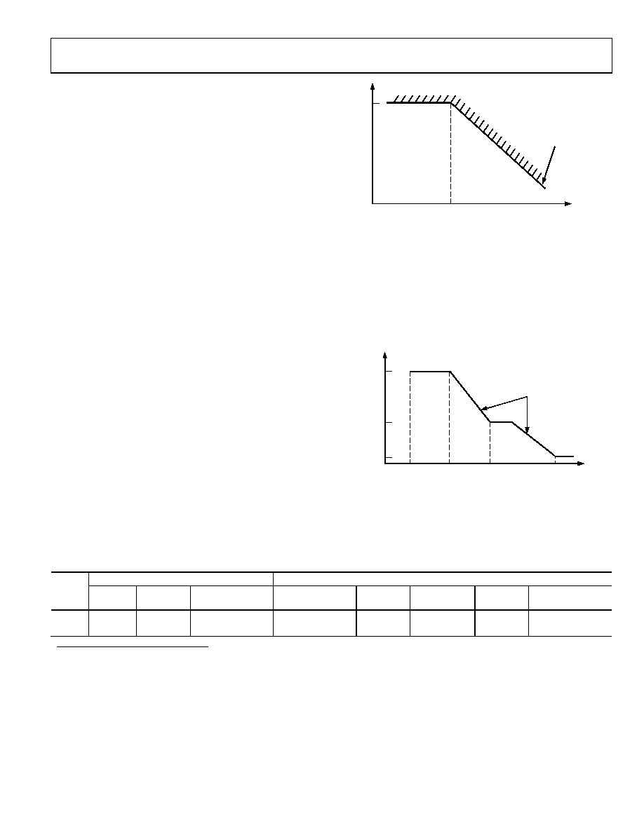
SLOPE = –20dB/DECADE
JITTER FREQUENCY (kHz)
0.1
J
ITTE
R
GAIN
(dB)
fC
ACCEPTABLE
RANGE
03877-0-011
Figure 11. Jitter Transfer Curve
Jitter Tolerance
The jitter tolerance is defined as the peak-to-peak amplitude of
the sinusoidal jitter applied on the input signal that causes a
1 dB power penalty. This is a stress test intended to ensure that
no additional penalty is incurred under the operating
conditions (Figure 12).
SLOPE = –20dB/DECADE
f0
f1
f2
f3
f4
JITTER FREQUENCY (Hz)
15
1.5
0.15
IN
P
U
T
J
ITTE
R
AMP
L
IT
UDE
(UI
)
03877-0-012
Figure 12. SONET Jitter Tolerance Mask
Table 4. Jitter Transfer and Tolerance: SONET Specifications vs. ADN2807
Jitter Transfer
Jitter Tolerance
Rate
SONET
Spec (fC)
ADN2807
(kHz)
Implementation
Margin
Mask Corner
Frequency (kHz)
ADN2807
SONET Spec
(UI p-p)
ADN2807
(UI p-p)
Implementation
Margin2
OC-12
500 kHz
140
3.6
250 kHz
4.8 MHz
0.15
1.0
6.67
OC-3
130 kHz
48
2.7
65 kHz
600 kHz
0.15
1.0
6.67
2 Jitter tolerance measurements are limited by test equipment capabilities.
相关PDF资料 |
PDF描述 |
|---|---|
| ADN2811ACPZ-CML | IC CLK/DATA REC W/AMP 48-LFCSP |
| ADN2812ACPZ-RL7 | IC CLOCK/DATA RECOVERY 32LFCSP |
| ADN2813ACPZ-500RL7 | IC CLK/DATA REC 1.25GBPS 32LFCSP |
| ADN2814ACPZ-500RL7 | IC CLK/DATA REC 675MBPS 32-LFCSP |
| ADN2815ACPZ | IC CLK/DATA REC 1.25GBPS 32LFCSP |
相关代理商/技术参数 |
参数描述 |
|---|---|
| ADN2807ACPZ-RL | 功能描述:IC CLOCK/DATA RECOVERY 48LFCSP RoHS:是 类别:集成电路 (IC) >> 时钟/计时 - 专用 系列:- 标准包装:28 系列:- 类型:时钟/频率发生器 PLL:是 主要目的:Intel CPU 服务器 输入:时钟 输出:LVCMOS 电路数:1 比率 - 输入:输出:3:22 差分 - 输入:输出:无/是 频率 - 最大:400MHz 电源电压:3.135 V ~ 3.465 V 工作温度:0°C ~ 85°C 安装类型:表面贴装 封装/外壳:64-TFSOP (0.240",6.10mm 宽) 供应商设备封装:64-TSSOP 包装:管件 |
| ADN2809 | 制造商:AD 制造商全称:Analog Devices 功能描述:Multi-Rate to 2.7Gbps Clock and Data Recovery IC with Limiting Amplifier |
| ADN2809XCP | 制造商:AD 制造商全称:Analog Devices 功能描述:Multi-Rate to 2.7Gbps Clock and Data Recovery IC with Limiting Amplifier |
| ADN2809XCP-RL | 制造商:AD 制造商全称:Analog Devices 功能描述:Multi-Rate to 2.7Gbps Clock and Data Recovery IC with Limiting Amplifier |
| ADN2811 | 制造商:AD 制造商全称:Analog Devices 功能描述:OC-48/OC-48 FEC Clock and Data Recovery IC with Integrated Limiting Amp |
发布紧急采购,3分钟左右您将得到回复。