参数资料
| 型号: | ADN2807ACPZ |
| 厂商: | Analog Devices Inc |
| 文件页数: | 6/20页 |
| 文件大小: | 0K |
| 描述: | IC CLOCK/DATA RECOVERY 48LFCSP |
| 标准包装: | 1 |
| 类型: | 时钟和数据恢复(CDR),多路复用器 |
| PLL: | 是 |
| 主要目的: | SONET/SDH,STM |
| 输入: | CML |
| 输出: | CML |
| 电路数: | 1 |
| 比率 - 输入:输出: | 1:2 |
| 差分 - 输入:输出: | 是/是 |
| 频率 - 最大: | 622MHz |
| 电源电压: | 3 V ~ 3.6 V |
| 工作温度: | -40°C ~ 85°C |
| 安装类型: | 表面贴装 |
| 封装/外壳: | 48-VFQFN 裸露焊盘,CSP |
| 供应商设备封装: | 48-LFCSP |
| 包装: | 托盘 |
ADN2807
Rev. A | Page 14 of 20
50
50
QUANTIZER
+
ADN2807
VREF
NIN
PIN
50
50
VCC
TDINP/N
LOOPEN
BYPASS
CDR
RETIMED
DATA
CLK
0
1
10
DATAOUTP/N
CLKOUTP/N SQUELCH
FROM
QUANTIZER
OUTPUT
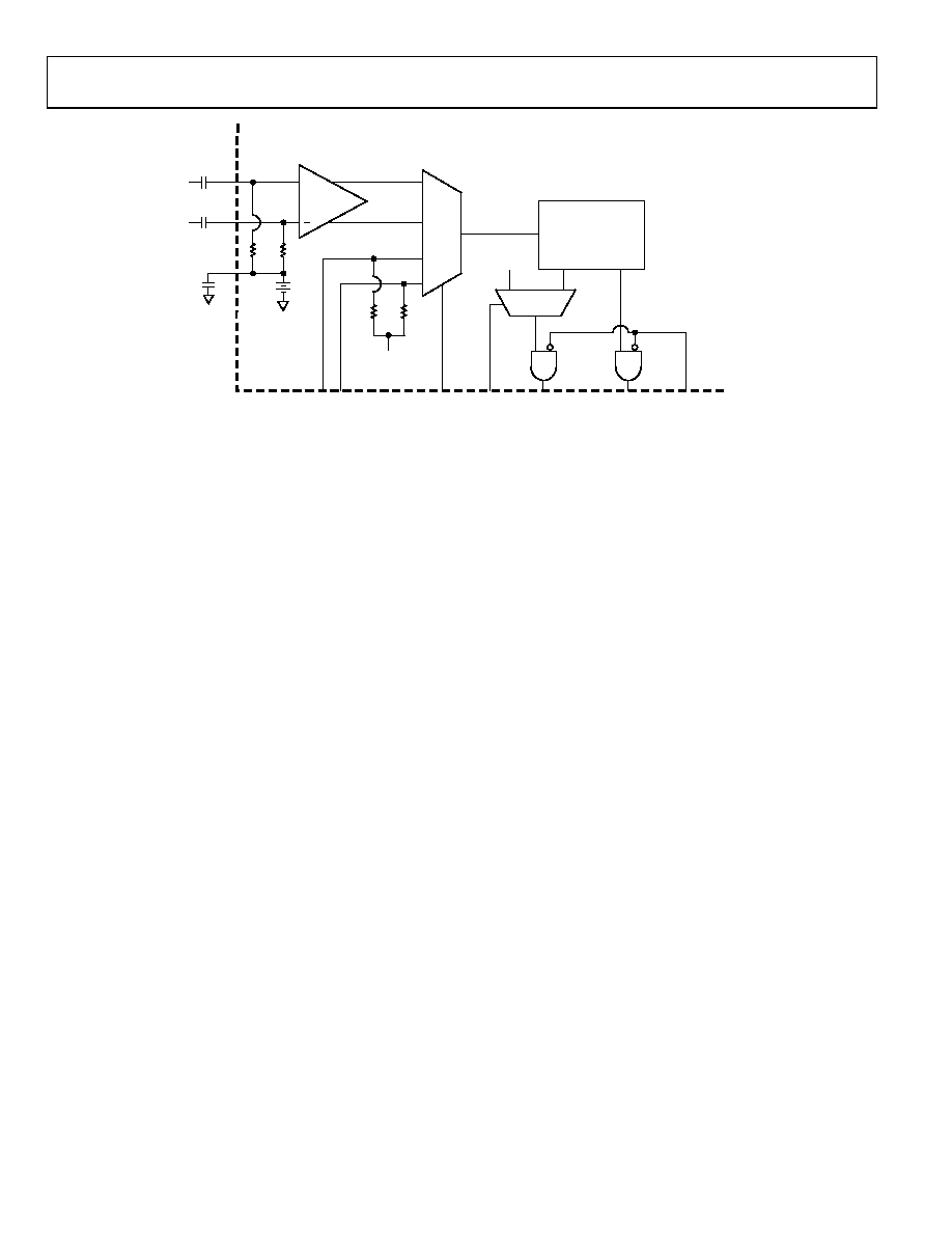
03877-0-019
Figure 19. Test Modes
SQUELCH MODE
When the squelch input is driven to a TTL high state, both the
clock and data outputs are set to the zero state to suppress
downstream processing. If desired, this pin can be directly
driven by the LOS (loss-of-signal) detector output (SDOUT). If
the squelch function is not required, the pin should be tied to
VEE.
TEST MODES—BYPASS AND LOOP-BACK
When the bypass input is driven to a TTL high state, the
quantizer output is connected directly to the buffers driving the
data out pins, thus bypassing the clock recovery circuit
(Figure 19). This feature can help the system to deal with
nonstandard bit rates.
The loopback mode can be invoked by driving the LOOPEN
pin to a TTL high state, which facilitates system diagnostic
testing. This will connect the test inputs (TDINP/N) to the
clock and data recovery circuit (per Figure 19). The test inputs
have internal 50 terminations and can be left floating when
not in use. TDINP/N are CML inputs and can be dc-coupled
only when being driven by CML outputs. The TDINP/N inputs
must be ac-coupled if driven by anything other than CML
outputs. Bypass and loop-back modes are mutually exclusive;
only one of these modes can be used at any given time. The
ADN2807 is put into an indeterminate state if both BYPASS
and LOOPEN pins are set to Logic 1 at the same time.
相关PDF资料 |
PDF描述 |
|---|---|
| ADN2811ACPZ-CML | IC CLK/DATA REC W/AMP 48-LFCSP |
| ADN2812ACPZ-RL7 | IC CLOCK/DATA RECOVERY 32LFCSP |
| ADN2813ACPZ-500RL7 | IC CLK/DATA REC 1.25GBPS 32LFCSP |
| ADN2814ACPZ-500RL7 | IC CLK/DATA REC 675MBPS 32-LFCSP |
| ADN2815ACPZ | IC CLK/DATA REC 1.25GBPS 32LFCSP |
相关代理商/技术参数 |
参数描述 |
|---|---|
| ADN2807ACPZ-RL | 功能描述:IC CLOCK/DATA RECOVERY 48LFCSP RoHS:是 类别:集成电路 (IC) >> 时钟/计时 - 专用 系列:- 标准包装:28 系列:- 类型:时钟/频率发生器 PLL:是 主要目的:Intel CPU 服务器 输入:时钟 输出:LVCMOS 电路数:1 比率 - 输入:输出:3:22 差分 - 输入:输出:无/是 频率 - 最大:400MHz 电源电压:3.135 V ~ 3.465 V 工作温度:0°C ~ 85°C 安装类型:表面贴装 封装/外壳:64-TFSOP (0.240",6.10mm 宽) 供应商设备封装:64-TSSOP 包装:管件 |
| ADN2809 | 制造商:AD 制造商全称:Analog Devices 功能描述:Multi-Rate to 2.7Gbps Clock and Data Recovery IC with Limiting Amplifier |
| ADN2809XCP | 制造商:AD 制造商全称:Analog Devices 功能描述:Multi-Rate to 2.7Gbps Clock and Data Recovery IC with Limiting Amplifier |
| ADN2809XCP-RL | 制造商:AD 制造商全称:Analog Devices 功能描述:Multi-Rate to 2.7Gbps Clock and Data Recovery IC with Limiting Amplifier |
| ADN2811 | 制造商:AD 制造商全称:Analog Devices 功能描述:OC-48/OC-48 FEC Clock and Data Recovery IC with Integrated Limiting Amp |
发布紧急采购,3分钟左右您将得到回复。