- 您现在的位置:买卖IC网 > PDF目录9375 > ADN2850BCPZ25 (Analog Devices Inc)IC RHEO DGTL 10B DL 25K 16LFCSP PDF资料下载
参数资料
| 型号: | ADN2850BCPZ25 |
| 厂商: | Analog Devices Inc |
| 文件页数: | 27/28页 |
| 文件大小: | 0K |
| 描述: | IC RHEO DGTL 10B DL 25K 16LFCSP |
| 产品变化通告: | Metal Edit Change 03/Feb/2012 |
| 标准包装: | 1 |
| 接片: | 1024 |
| 电阻(欧姆): | 25k |
| 电路数: | 2 |
| 温度系数: | 标准值 35 ppm/°C |
| 存储器类型: | 非易失 |
| 接口: | 4 线 SPI(芯片选择) |
| 电源电压: | 3 V ~ 5.5 V,±2.25 V ~ 2.75 V |
| 工作温度: | -40°C ~ 85°C |
| 安装类型: | 表面贴装 |
| 封装/外壳: | 16-VQFN 裸露焊盘,CSP |
| 供应商设备封装: | 16-LFCSP |
| 包装: | 托盘 |
第1页第2页第3页第4页第5页第6页第7页第8页第9页第10页第11页第12页第13页第14页第15页第16页第17页第18页第19页第20页第21页第22页第23页第24页第25页第26页当前第27页第28页
ADN2850
Data Sheet
Rev. E | Page 8 of 28
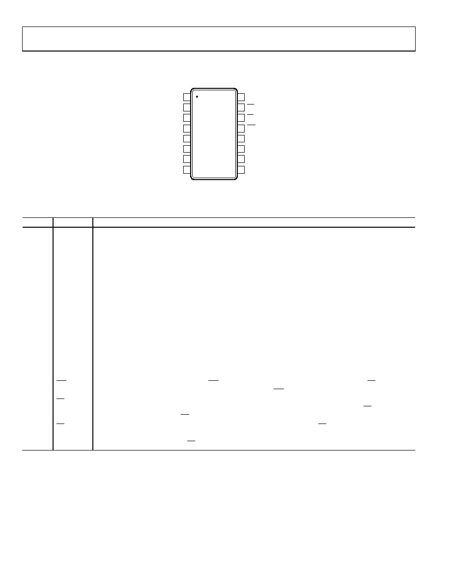
PIN CONFIGURATION AND FUNCTION DESCRIPTIONS
SDI
SDO
GND
V1
VSS
W1
CLK
B1
CS
PR
WP
VDD
V2
W2
B2
RDY
1
2
3
4
5
6
7
8
16
15
14
13
12
11
10
9
ADN2850
TOP VIEW
(Not to Scale)
0
2
6
0
-0
0
5
Figure 4. Pin Configuration
Table 4. Pin Function Descriptions
Pin No.
Mnemonic
Description
1
CLK
Serial Input Register Clock. Shifts in one bit at a time on positive clock edges.
2
SDI
Serial Data Input. Shifts in one bit at a time on positive clock CLK edges. MSB loads first.
3
SDO
Serial Data Output. Serves readback and daisy-chain functions. Command 9 and Command 10 activate the SDO
output for the readback function, delayed by 24 or 25 clock pulses, depending on the clock polarity before and
after the data-word (see Figure 2 and Figure 3). In other commands, the SDO shifts out the previously loaded SDI
bit pattern, delayed by 24 or 25 clock pulses depending on the clock polarity (see Figure 2 and Figure 3). This
previously shifted out SDI can be used for daisy-chaining multiple devices. Whenever SDO is used, a pull-up
resistor in the range of 1 k to 10 k is needed.
4
GND
Ground Pin, Logic Ground Reference.
5
VSS
Negative Supply. Connect to 0 V for single-supply applications. If VSS is used in dual supply, it must be able to sink
2 mA for 15 ms when storing data to EEMEM.
6
V1
Log Output Voltage 1. Generates voltage from an internal diode configured transistor.
7
W1
Wiper Terminal of RDAC1. ADDR (RDAC1) = 0x0.
8
B1
Terminal B of RDAC1.
9
B2
Terminal B of RDAC2.
10
W2
Wiper terminal of RDAC2. ADDR (RDAC2) = 0x1.
11
V2
Log Output Voltage 2. Generates voltage from an internal diode configured transistor.
12
VDD
Positive Power Supply.
13
AA
WPEE
Optional Write Protect. When active low,
AA
WPEE
AA
prevents any changes to the present contents, except
AA
PREE
AA
strobe.
CMD_1 and COMD_8 refresh the RDAC register from EEMEM. Tie
AA
WPEE
AA
to VDD, if not used.
14
AA
PREE
Optional Hardware Override Preset. Refreshes the scratchpad register with current contents of the EEMEM
register. Factory default loads midscale 51210 until EEMEM is loaded with a new value by the user.
AA
PREE
AA
is activated
at the logic high transition. Tie
AA
PREE
AA
to VDD, if not used.
15
AA
CSEE
Serial Register Chip Select Active Low. Serial register operation takes place when
AA
CSEE
AA
returns to logic high.
16
RDY
Ready. Active high open-drain output. Identifies completion of Instruction 2, Instruction 3, Instruction 8,
Instruction 9, Instruction 10, and
AA
PREE
AA
.
相关PDF资料 |
PDF描述 |
|---|---|
| VE-B3K-MY-F1 | CONVERTER MOD DC/DC 40V 50W |
| ADN2850BCPZ250 | IC DGTL RHEO DL 1024POS 16LFCSP |
| VE-B3J-MY-F4 | CONVERTER MOD DC/DC 36V 50W |
| AD5232BRU10 | IC DGTL POT 256POS 10K 16TSSOP |
| VI-2NW-MX-B1 | CONVERTER MOD DC/DC 5.5V 75W |
相关代理商/技术参数 |
参数描述 |
|---|---|
| ADN2850BCPZ250 | 功能描述:IC DGTL RHEO DL 1024POS 16LFCSP RoHS:是 类别:集成电路 (IC) >> 数据采集 - 数字电位器 系列:- 标准包装:3,300 系列:WiperLock™ 接片:257 电阻(欧姆):100k 电路数:1 温度系数:标准值 150 ppm/°C 存储器类型:易失 接口:3 线 SPI(芯片选择) 电源电压:1.8 V ~ 5.5 V 工作温度:-40°C ~ 125°C 安装类型:表面贴装 封装/外壳:8-VDFN 裸露焊盘 供应商设备封装:8-DFN-EP(3x3) 包装:带卷 (TR) |
| ADN2850BCPZ250-RL7 | 功能描述:IC DGTL RHEO DL 25K 9BIT16LFCSP RoHS:是 类别:集成电路 (IC) >> 数据采集 - 数字电位器 系列:- 标准包装:3,000 系列:DPP 接片:32 电阻(欧姆):10k 电路数:1 温度系数:标准值 300 ppm/°C 存储器类型:非易失 接口:3 线串行(芯片选择,递增,增/减) 电源电压:2.5 V ~ 6 V 工作温度:-40°C ~ 85°C 安装类型:表面贴装 封装/外壳:8-WFDFN 裸露焊盘 供应商设备封装:8-TDFN(2x3) 包装:带卷 (TR) |
| ADN2850BCPZ25-RL7 | 功能描述:IC DGTL RHEO DL 25K 9BIT16LFCSP RoHS:是 类别:集成电路 (IC) >> 数据采集 - 数字电位器 系列:- 标准包装:3,000 系列:DPP 接片:32 电阻(欧姆):10k 电路数:1 温度系数:标准值 300 ppm/°C 存储器类型:非易失 接口:3 线串行(芯片选择,递增,增/减) 电源电压:2.5 V ~ 6 V 工作温度:-40°C ~ 85°C 安装类型:表面贴装 封装/外壳:8-WFDFN 裸露焊盘 供应商设备封装:8-TDFN(2x3) 包装:带卷 (TR) |
| ADN2850BRU25 | 制造商:Analog Devices 功能描述: |
| adn2850bru25-rl7 | 制造商:Analog Devices 功能描述: |
发布紧急采购,3分钟左右您将得到回复。