- 您现在的位置:买卖IC网 > PDF目录1899 > ADN4668ARZ-REEL7 (Analog Devices Inc)IC RCVR LVDS DIFF 4CH 16SOIC PDF资料下载
参数资料
| 型号: | ADN4668ARZ-REEL7 |
| 厂商: | Analog Devices Inc |
| 文件页数: | 7/12页 |
| 文件大小: | 0K |
| 描述: | IC RCVR LVDS DIFF 4CH 16SOIC |
| 标准包装: | 1,000 |
| 类型: | 线路接收器 |
| 驱动器/接收器数: | 0/4 |
| 规程: | LVDS |
| 电源电压: | 3 V ~ 3.6 V |
| 安装类型: | 表面贴装 |
| 封装/外壳: | 16-SOIC(0.154",3.90mm 宽) |
| 供应商设备封装: | 16-SOIC |
| 包装: | 带卷 (TR) |
ADN4668
Rev. A | Page 4 of 12
AC CHARACTERISTICS
VDD = 3.0 V to 3.6 V, CL = 15 pF to GND, all specifications TMIN to TMAX, unless otherwise noted.1, 2, 3, 4
Table 2.
Parameter5
Min
Typ
Max
Unit
Conditions/Comments6
Differential Propagation Delay, High-to-Low, tPHLD
1.2
2.0
2.7
ns
Differential Propagation Delay, Low-to-High, tPLHD
1.2
1.9
2.7
ns
0
0.1
0.4
ns
Differential Channel-to-Channel Skew, Same Device, tSKD23
0
0.15
0.5
ns
Differential Part-to-Part Skew, tSKD34
1.0
ns
Differential Part-to-Part Skew, tSKD49
1.5
ns
Rise Time, tTLH
0.5
1.0
ns
Fall Time, tTHL
0.35
1.0
ns
Disable Time, High-to-Z, tPHZ
8
14
ns
Disable Time, Low-to-Z, tPLZ
8
14
ns
Enable Time, Z-to-High, tPZH
9
14
ns
Enable Time, Z-to-Low, tPZL
9
14
ns
Maximum Operating Frequency, fMAX10
200
250
MHz
All channels switching
1 All typicals are given for VCC = 3.3 V and TA = 25°C.
2 Generator waveform for all tests, unless otherwise specified: f = 1 MHz, ZO = 50 Ω, and tR and tF (0% to 100%) ≤ 3 ns for RINx+/RINx.
3 Channel-to-channel skew, tSKD2, is defined as the difference between the propagation delay of one channel and that of the others on the same chip with any event on
the inputs.
4 Part-to-part skew, tSKD3, is the differential channel-to-channel skew of any event between devices. This specification applies to devices at the same VCC and within 5°C of
each other within the operating temperature range.
5 AC parameters are guaranteed by design and characterization.
6 Current-into-device pins are defined as positive. Current-out-of-device pins are defined as negative. All voltages are referenced to ground, unless otherwise specified.
7 CL includes probe and jig capacitance.
8 tSKD1 is the magnitude difference in the differential propagation delay time between the positive-going edge and the negative-going edge of the same channel.
9 Part-to-part skew, tSKD4, is the differential channel-to-channel skew of any event between devices. This specification applies to devices over the recommended
operating temperature and voltage ranges and across process distribution. tSKD4 is defined as |maximum minimum| differential propagation delay.
10 fMAX generator input conditions: f = 200 MHz, tR = tF < 1 ns (0% to 100%), 50% duty cycle, differential (1.05 V p-p to 1.35 V p-p). Output criteria: 60%/40% duty cycle,
VOL (maximum = 0.4 V), VOH (minimum = 2.7 V), CL = 15 pF (stray plus probes).
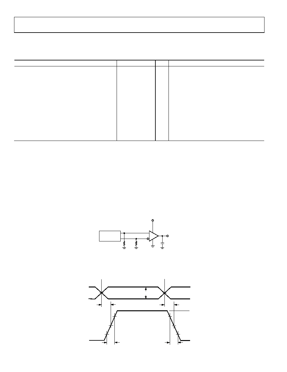
TEST CIRCUITS AND WAVEFORMS
SIGNAL
GENERATOR
RECEIVER
IS ENABLED
RINx+
RINx–
CL
CL = LOAD AND TEST JIG CAPACITANCE
VCC
ROUTx
50
07
23
7-
0
02
Figure 2. Test Circuit for Receiver Propagation Delay and Transition Time
80%
20%
1.5V
20%
1.5V
tPLHD
tPHLD
RINx–
RINx+
0V (DIFFERENTIAL)
tTLH
tTHL
VOH
VOL
1.2V
1.3V
1.1V
ROUTx
VID = 200mV
07
23
7-
0
03
Figure 3. Receiver Propagation Delay and Transition Time Waveforms
相关PDF资料 |
PDF描述 |
|---|---|
| ADN4690EBRZ | IC INTERFACE TXRX |
| ADN4693EBRZ-RL7 | IC TXRX MLVDS 200MBPS 14SOIC |
| ADN4695EBRZ-RL7 | IC TXRX MLVDS 100MBPS 14SOIC |
| ADN4697EBRZ | IC RCVR LVDS 2CH 14SOIC |
| ADN8102ACPZ-R7 | IC EQUALIZER 4CH XSTREAM 64LFCSP |
相关代理商/技术参数 |
参数描述 |
|---|---|
| ADN4668ARZ-REEL71 | 制造商:AD 制造商全称:Analog Devices 功能描述:3 V LVDS Quad CMOS Differential Line Receiver |
| ADN4670 | 制造商:AD 制造商全称:Analog Devices 功能描述:Programmable Low Voltage 1:10 LVDS Clock Driver |
| ADN4670BCPZ | 功能描述:IC CLOCK BUFFER MUX 2:10 16LFCSP RoHS:是 类别:集成电路 (IC) >> 时钟/计时 - 时钟缓冲器,驱动器 系列:- 产品培训模块:High Bandwidth Product Overview 标准包装:1,000 系列:Precision Edge® 类型:扇出缓冲器(分配) 电路数:1 比率 - 输入:输出:1:4 差分 - 输入:输出:是/是 输入:CML,LVDS,LVPECL 输出:CML 频率 - 最大:2.5GHz 电源电压:2.375 V ~ 2.625 V 工作温度:-40°C ~ 85°C 安装类型:表面贴装 封装/外壳:16-VFQFN 裸露焊盘,16-MLF? 供应商设备封装:16-MLF?(3x3) 包装:带卷 (TR) |
| ADN4670BCPZ-REEL7 | 功能描述:IC CLOCK BUFFER MUX 2:10 16LFCSP RoHS:是 类别:集成电路 (IC) >> 时钟/计时 - 时钟缓冲器,驱动器 系列:- 标准包装:74 系列:- 类型:扇出缓冲器(分配) 电路数:1 比率 - 输入:输出:1:10 差分 - 输入:输出:是/是 输入:HCSL, LVCMOS, LVDS, LVPECL, LVTTL 输出:HCSL,LVDS 频率 - 最大:400MHz 电源电压:3 V ~ 3.6 V 工作温度:-40°C ~ 85°C 安装类型:表面贴装 封装/外壳:32-VFQFN 裸露焊盘 供应商设备封装:32-QFN(5x5) 包装:管件 |
| ADN4670BSTZ | 功能描述:IC CLOCK BUFFER MUX 2:10 32LQFP RoHS:是 类别:集成电路 (IC) >> 时钟/计时 - 时钟缓冲器,驱动器 系列:- 标准包装:74 系列:- 类型:扇出缓冲器(分配) 电路数:1 比率 - 输入:输出:1:10 差分 - 输入:输出:是/是 输入:HCSL, LVCMOS, LVDS, LVPECL, LVTTL 输出:HCSL,LVDS 频率 - 最大:400MHz 电源电压:3 V ~ 3.6 V 工作温度:-40°C ~ 85°C 安装类型:表面贴装 封装/外壳:32-VFQFN 裸露焊盘 供应商设备封装:32-QFN(5x5) 包装:管件 |
发布紧急采购,3分钟左右您将得到回复。