- 您现在的位置:买卖IC网 > PDF目录1776 > ADP1111ANZ-12 (Analog Devices Inc)IC REG BUCK BST INV 12V .2A 8DIP PDF资料下载
参数资料
| 型号: | ADP1111ANZ-12 |
| 厂商: | Analog Devices Inc |
| 文件页数: | 11/15页 |
| 文件大小: | 0K |
| 描述: | IC REG BUCK BST INV 12V .2A 8DIP |
| 标准包装: | 50 |
| 类型: | 降压(降压),升压(升压),反相 |
| 输出类型: | 固定 |
| 输出数: | 1 |
| 输出电压: | 12V |
| 输入电压: | 2 V ~ 30 V |
| 频率 - 开关: | 72kHz |
| 电流 - 输出: | 200mA |
| 同步整流器: | 无 |
| 工作温度: | -40°C ~ 85°C |
| 安装类型: | 通孔 |
| 封装/外壳: | 8-DIP(0.300",7.62mm) |
| 包装: | 管件 |
| 供应商设备封装: | 8-PDIP |
�� �
�
�ADP1111�
�Table� I.� Component� Selection� for� Typical� Converters�
�Input�
�Output�
�Output�
�Circuit�
�Inductor�
�Inductor�
�Capacitor�
�Voltage�
�2� to� 3.1�
�2� to� 3.1�
�2� to� 3.1�
�2� to� 3.1�
�5�
�5�
�6.5� to� 11�
�12� to� 20�
�20� to� 30�
�5�
�12�
�Voltage�
�5�
�5�
�12�
�12�
�12�
�12�
�5�
�5�
�5�
�–5�
�–5�
�Current� (mA)�
�90� mA�
�10� mA�
�30� mA�
�10� mA�
�90� MA�
�30� mA�
�50� mA�
�300� mA�
�300� mA�
�7� mA�
�250� mA�
�Figure�
�4�
�4�
�4�
�4�
�4�
�4�
�5�
�5�
�5�
�6�
�6�
�Value�
�15� μ� H�
�47� μ� H�
�15� μ� H�
�47� μ� H�
�33� μ� H�
�47� μ� H�
�15� μ� H�
�56� μ� H�
�120� μ� H�
�56� μ� H�
�120� μ� H�
�Part� No.�
�CD75-150K�
�CTX50-1�
�CD75-150K�
�CTX50-1�
�CD75-330K�
�CTX50-1�
�CTX50-4�
�CTX100-4�
�CTX50-4�
�CTX100-4�
�Value�
�33� μ� F�
�10� μ� F�
�22� μ� F�
�10� μ� F�
�22� μ� F�
�15� μ� F�
�47� μ� F�
�47� μ� F�
�47� μ� F�
�47� μ� F�
�100� μ� F�
�Notes�
�*�
�**�
�**�
�**�
�**�
�NOTES�
�CD� =� Sumida.�
�CTX� =� Coiltronics.�
�*� *Add� 47� Ω� from� I� LIM� to� V� IN� .�
�**Add� 220� Ω� from� I� LIM� to� V� IN� .�
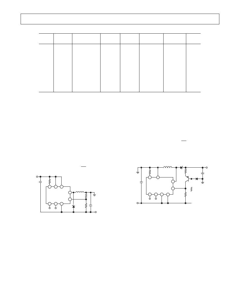
�POSITIVE-TO-NEGATIVE� CONVERSION�
�The� ADP1111� can� convert� a� positive� input� voltage� to� a� negative�
�output� voltage� as� shown� in� Figure� 22.� This� circuit� is� essentially�
�identical� to� the� step-down� application� of� Figure� 19,� except� that�
�also� reduces� the� circuit’s� output� voltage� sensitivity� to� tempera-�
�ture,� which� otherwise� would� be� dominated� by� the� –2� mV� V� BE�
�contribution� of� Q1.� The� output� voltage� for� this� circuit� is�
�determined� by� the� formula:�
�the� “output”� side� of� the� inductor� is� connected� to� power� ground.�
�When� the� ADP1111’s� internal� power� switch� turns� off,� current�
�V� OUT� =� 1.25� V� ?�
�R� 2�
�R� 1�
�flowing� in� the� inductor� forces� the� output� (–V� OUT� )� to� a� negative�
�potential.� The� ADP1111� will� continue� to� turn� the� switch� on�
�until� its� FB� pin� is� 1.25� V� above� its� GND� pin,� so� the� output�
�voltage� is� determined� by� the� formula:�
�Unlike� the� positive� step-up� converter,� the� negative-to-positive�
�converter’s� output� voltage� can� be� either� higher� or� lower� than� the�
�input� voltage.�
�V� OUT� =� 1.25� V� ?� ?� 1� +�
�INPUT�
�+�
�C� INPUT�
�R� LIM�
�?�
�?�
�R� 2� ?�
�R� 1� ?� ?�
�+�
�C2�
�R� LIM�
�1�
�I� LIM�
�2�
�V� IN�
�L1�
�SW1� 3�
�D1�
�1N5818�
�R2�
�Q1�
�MJE210�
�+�
�D2�
�2N3906�
�C� L�
�POSITIVE�
�OUTPUT�
�1� 2� 3�
�I� LIM� V� IN� SW1�
�ADP1111�
�SW2� 4�
�L1�
�R2�
�OUTPUT�
�ADP1111�
�FB� 8�
�AO� SET� GND� SW2�
�6� 7� 5� 4�
�R1�
�10k� Ω�
�FB� 8�
�AO� SET� GND�
�6� 7� 5�
�D1�
�1N5818�
�R1�
�+�
�C� L�
�NEGATIVE�
�INPUT�
�NC�
�NC�
�NC�
�NC�
�NEGATIVE�
�OUTPUT�
�Figure� 23.� ADP1111� Negative-to-Positive� Converter�
�Figure� 22.� Positive-to-Negative� Converter�
�The� design� criteria� for� the� step-down� application� also� apply� to�
�the� positive-to-negative� converter.� The� output� voltage� should� be�
�limited� to� |6.2� V|� unless� a� diode� is� inserted� in� series� with� the�
�SW2� pin� (see� Figure� 20.)� Also,� D1� must� again� be� a� Schottky�
�diode� to� prevent� excessive� power� dissipation� in� the� ADP1111.�
�NEGATIVE-TO-POSITIVE� CONVERSION�
�The� circuit� of� Figure� 23� converts� a� negative� input� voltage� to� a�
�positive� output� voltage.� Operation� of� this� circuit� configuration� is�
�similar� to� the� step-up� topology� of� Figure� 18,� except� the� current�
�through� feedback� resistor� R2� is� level-shifted� below� ground� by� a�
�PNP� transistor.� The� voltage� across� R2� is� V� OUT� –V� BEQ1� .� How-�
�ever,� diode� D2� level-shifts� the� base� of� Q1� about� 0.6� V� below�
�ground� thereby� cancelling� the� V� BE� of� Q1.� The� addition� of� D2�
�0�
�REV.� A�
�LIMITING� THE� SWITCH� CURRENT�
�The� ADP1111’s� R� LIM� pin� permits� the� switch� current� to� be�
�limited� with� a� single� resistor.� This� current� limiting� action� occurs�
�on� a� pulse� by� pulse� basis.� This� feature� allows� the� input� voltage�
�to� vary� over� a� wide� range� without� saturating� the� inductor� or�
�exceeding� the� maximum� switch� rating.� For� example,� a� particular�
�design� may� require� peak� switch� current� of� 800� mA� with� a� 2.0� V�
�input.� If� V� IN� rises� to� 4� V,� however,� the� switch� current� will�
�exceed� 1.6� A.� The� ADP1111� limits� switch� current� to� 1.5� A� and�
�thereby� protects� the� switch,� but� the� output� ripple� will� increase.�
�Selecting� the� proper� resistor� will� limit� the� switch� current� to�
�800� mA,� even� if� V� IN� increases.� The� relationship� between� R� LIM�
�and� maximum� switch� current� is� shown� in� Figure� 6.�
�The� I� LIM� feature� is� also� valuable� for� controlling� inductor� current�
�when� the� ADP1111� goes� into� continuous-conduction� mode.�
�–11� –�
�相关PDF资料 |
PDF描述 |
|---|---|
| ADP121-ACBZ12R7 | IC REG LDO 1.2V .15A 4WLCSP |
| ADP122AUJZ-2.9-R7 | IC REG LDO 2.9V .3A 5TSOT |
| ADP124ARHZ-2.85-R7 | IC REG LDO 2.85V .5A 8MSOP |
| ADP130AUJZ-2.5-R7 | IC REG LDO 2.5V .35A TSOT-23-5 |
| ADP150AUJZ-2.5-R7 | IC REG LDO 2.5V .15A TSOT-5 |
相关代理商/技术参数 |
参数描述 |
|---|---|
| ADP1111ANZ-3.3 | 功能描述:IC REG BUCK BOOST INV 3.3V 8DIP RoHS:是 类别:集成电路 (IC) >> PMIC - 稳压器 - DC DC 开关稳压器 系列:- 标准包装:2,500 系列:- 类型:降压(降压) 输出类型:固定 输出数:1 输出电压:1.2V,1.5V,1.8V,2.5V 输入电压:2.7 V ~ 20 V PWM 型:- 频率 - 开关:- 电流 - 输出:50mA 同步整流器:是 工作温度:-40°C ~ 125°C 安装类型:表面贴装 封装/外壳:10-TFSOP,10-MSOP(0.118",3.00mm 宽)裸露焊盘 包装:带卷 (TR) 供应商设备封装:10-MSOP 裸露焊盘 |
| ADP1111ANZ-5 | 功能描述:IC REG BUCK BST INV 5V 0.2A 8DIP RoHS:是 类别:集成电路 (IC) >> PMIC - 稳压器 - DC DC 开关稳压器 系列:- 标准包装:250 系列:- 类型:降压(降压) 输出类型:固定 输出数:1 输出电压:1.2V 输入电压:2.05 V ~ 6 V PWM 型:电压模式 频率 - 开关:2MHz 电流 - 输出:500mA 同步整流器:是 工作温度:-40°C ~ 85°C 安装类型:表面贴装 封装/外壳:6-UFDFN 包装:带卷 (TR) 供应商设备封装:6-SON(1.45x1) 产品目录页面:1032 (CN2011-ZH PDF) 其它名称:296-25628-2 |
| ADP1111AR | 制造商:Analog Devices 功能描述:Conv DC-DC Single Non-Inv/Inv/Step Up/Step Down 2V to 30V 8-Pin SOIC N 制造商:Analog Devices 功能描述:CONV DC-DC SGL-OUT NON-INV/INV/STEP UP/STEP DOWN 8SOIC N - Rail/Tube 制造商:Analog Devices 功能描述:IC SWITCHING REGULATOR |
| ADP1111AR-12 | 制造商:Analog Devices 功能描述:Conv DC-DC Single Non-Inv/Inv/Step Up/Step Down 2V to 30V 8-Pin SOIC N 制造商:Rochester Electronics LLC 功能描述:MICROPOWER STEP-UP/DOWN SWITCHING REG. - Bulk |
| ADP1111AR-12-REEL | 制造商:Analog Devices 功能描述:Conv DC-DC Single Non-Inv/Inv/Step Up/Step Down 2V to 30V 8-Pin SOIC N T/R |
发布紧急采购,3分钟左右您将得到回复。