- 您现在的位置:买卖IC网 > PDF目录16945 > ADP1755-EVALZ (Analog Devices Inc)BOARD EVAL 1.2V SET ADP1755 PDF资料下载
参数资料
| 型号: | ADP1755-EVALZ |
| 厂商: | Analog Devices Inc |
| 文件页数: | 5/20页 |
| 文件大小: | 0K |
| 描述: | BOARD EVAL 1.2V SET ADP1755 |
| 标准包装: | 1 |
| 每 IC 通道数: | 1 - 单 |
| 输出电压: | 0.75 ~ 3V |
| 电流 - 输出: | 1.2A |
| 输入电压: | 1.6 ~ 3.6V |
| 稳压器类型: | 正,可调式 |
| 工作温度: | -40°C ~ 125°C |
| 板类型: | 完全填充 |
| 已供物品: | 板 |
| 已用 IC / 零件: | ADP1755 |
�� ��
��
��Data� Sheet�
�ABSOLUTE� MAXIMUM� RATINGS�
�Table� 3.�
�Parameter� Rating�
�VIN� to� GND� ?0.3� V� to� +4.0� V�
�VOUT� to� GND� ?0.3� V� to� VIN�
�EN� to� GND� ?0.3� V� to� VIN�
�SS� to� GND� ?0.3� V� to� VIN�
�PG� to� GND� ?0.3� V� to� +4.0� V�
�SENSE/ADJ� to� GND� ?0.3� V� to� VIN�
�Storage� Temperature� Range� ?65°C� to� +150°C�
�Junction� Temperature� Range� ?40°C� to� +125°C�
�Junction� Temperature� 150°C�
�Soldering� Conditions� JEDEC� J-STD-020�
�Stresses� above� those� listed� under� Absolute� Maximum� Ratings�
�may� cause� permanent� damage� to� the� device.� This� is� a� stress�
�rating� only;� functional� operation� of� the� device� at� these� or� any�
�other� conditions� above� those� indicated� in� the� operational�
�section� of� this� specification� is� not� implied.� Exposure� to� absolute�
�maximum� rating� conditions� for� extended� periods� may� affect�
�device� reliability.�
�THERMAL� DATA�
�Absolute� maximum� ratings� apply� individually� only,� not� in�
�combination.� The� ADP1754/ADP1755� may� be� damaged� if� the�
�junction� temperature� limits� are� exceeded.� Monitoring� ambient�
�temperature� does� not� guarantee� that� T� J� is� within� the� specified�
�temperature� limits.� In� applications� with� high� power� dissipation�
�and� poor� thermal� resistance,� the� maximum� ambient� temperature�
�may� need� to� be� derated.� In� applications� with� moderate� power�
�dissipation� and� low� PCB� thermal� resistance,� the� maximum�
�ambient� temperature� can� exceed� the� maximum� limit� as� long�
�as� the� junction� temperature� is� within� specification� limits.�
�The� junction� temperature� (T� J� )� of� the� device� is� dependent� on� the�
�ADP1754/ADP1755�
�Junction-to-ambient� thermal� resistance� (θ� JA� )� of� the� package� is�
�based� on� modeling� and� calculation� using� a� 4-layer� board.� The�
�junction-to-ambient� thermal� resistance� is� highly� dependent�
�on� the� application� and� board� layout.� In� applications� where� high�
�maximum� power� dissipation� exists,� close� attention� to� thermal�
�board� design� is� required.� The� value� of� θ� JA� may� vary,� depending�
�on� PCB� material,� layout,� and� environmental� conditions.� The�
�specified� values� of� θ� JA� are� based� on� a� 4-layer,� 4� in� ×� 3� in� circuit�
�board.� Refer� to� JEDEC� JESD51-7� for� detailed� information� about�
�board� construction.� For� more� information,� see� the� AN-772�
��Lead� Frame� Chip� Scale� Package� (LFCSP)� .�
�Ψ� JB� is� the� junction-to-board� thermal� characterization� parameter�
�with� units� of� °C/W.� Ψ� JB� of� the� package� is� based� on� modeling� and�
�calculation� using� a� 4-layer� board.� The� JESD51-12� document,�
�Guidelines� for� Reporting� and� Using� Electronic� Package� Thermal�
�Information� ,� states� that� thermal� characterization� parameters� are�
�not� the� same� as� thermal� resistances.� Ψ� JB� measures� the� component�
�power� flowing� through� multiple� thermal� paths� rather� than� through�
�a� single� path� as� in� thermal� resistance,� θ� JB� .� Therefore,� Ψ� JB� thermal�
�paths� include� convection� from� the� top� of� the� package� as� well� as�
�radiation� from� the� package,� factors� that� make� Ψ� JB� more� useful� in�
�real-world� applications.� Maximum� junction� temperature� (T� J� )�
�is� calculated� from� the� board� temperature� (T� B� )� and� the� power�
�dissipation� (P� D� )� using� the� following� formula:�
�T� J� =� T� B� +� (� P� D� ×� Ψ� JB� )�
�Refer� to� the� JEDEC� JESD51-8� and� JESD51-12� documents� for� more�
�detailed� information� about� Ψ� JB� .�
�THERMAL� RESISTANCE�
�θ� JA� and� Ψ� JB� are� specified� for� the� worst-case� conditions,� that� is,� a�
�device� soldered� in� a� circuit� board� for� surface-mount� packages.�
�ambient� temperature� (T� A� ),� the� power� dissipation� of� the� device�
�(P� D� ),� and� the� junction-to-ambient� thermal� resistance� of� the�
�package� (θ� JA� ).� T� J� is� calculated� using� the� following� formula:�
�T� J� =� T� A� +� (� P� D� ×� θ� JA� )�
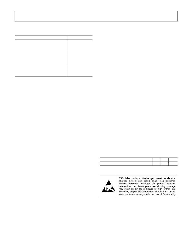
�Table� 4.� Thermal� Resistance�
�Package� Type�
�16-Lead� LFCSP� with� Exposed� Pad� (CP-16-4)�
�θ� JA�
�42�
�Ψ� JB�
�25.5�
�Unit�
�°C/W�
�ESD� CAUTION�
�Rev.� F� |� Page� 5� of� 20�
�相关PDF资料 |
PDF描述 |
|---|---|
| ADP1741-EVALZ | BOARD EVAL 2A ADP1741 |
| ADP170-1.8-EVALZ | BOARD EVAL ADP170 1.8V |
| ADP171-EVALZ | BOARD EVAL ADP171 1V |
| VE-JVM-EY | CONVERTER MOD DC/DC 10V 50W |
| VI-24L-EY | CONVERTER MOD DC/DC 28V 50W |
相关代理商/技术参数 |
参数描述 |
|---|---|
| ADP175ARMZ-0.75R7 | 制造商:AD 制造商全称:Analog Devices 功能描述:500 mA, Low Dropout, CMOS Linear Regulator |
| ADP175ARMZ-0.85R7 | 制造商:AD 制造商全称:Analog Devices 功能描述:500 mA, Low Dropout, CMOS Linear Regulator |
| ADP175ARMZ-0.8-R7 | 制造商:AD 制造商全称:Analog Devices 功能描述:500 mA, Low Dropout, CMOS Linear Regulator |
| ADP175ARMZ-0.95R7 | 制造商:AD 制造商全称:Analog Devices 功能描述:500 mA, Low Dropout, CMOS Linear Regulator |
| ADP175ARMZ-0.9-R7 | 制造商:AD 制造商全称:Analog Devices 功能描述:500 mA, Low Dropout, CMOS Linear Regulator |
发布紧急采购,3分钟左右您将得到回复。