- 您现在的位置:买卖IC网 > PDF目录17413 > ADP1823-EVAL (Analog Devices Inc)BOARD EVAL FOR ADP1823 PDF资料下载
参数资料
| 型号: | ADP1823-EVAL |
| 厂商: | Analog Devices Inc |
| 文件页数: | 20/32页 |
| 文件大小: | 0K |
| 描述: | BOARD EVAL FOR ADP1823 |
| 标准包装: | 1 |
| 主要目的: | DC/DC,步降 |
| 输出及类型: | 1,非隔离 |
| 输出电压: | 1.2V |
| 电流 - 输出: | 15A |
| 输入电压: | 5.5 ~ 20 V |
| 稳压器拓扑结构: | 降压 |
| 频率 - 开关: | 300kHz |
| 板类型: | 完全填充 |
| 已供物品: | 板 |
| 已用 IC / 零件: | ADP1823 |
| 产品目录页面: | 791 (CN2011-ZH PDF) |
第1页第2页第3页第4页第5页第6页第7页第8页第9页第10页第11页第12页第13页第14页第15页第16页第17页第18页第19页当前第20页第21页第22页第23页第24页第25页第26页第27页第28页第29页第30页第31页第32页
�� �
�
�ADP1823�
�The� rest� of� the� system� gain� is� needed� to� reach� 0� dB� at� crossover.�
�The� total� gain� of� the� system,� therefore,� is� given� by�
�GAIN�
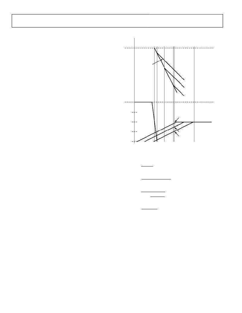
�LC� FILTER� BODE� PLOT�
�PHASE� CONTRIBUTION� AT� CROSSOVER�
�OF� VARIOUS� ESR� ZERO� CORNERS�
�A� T� =� A� MOD� +� A� FILTER� +� A� COMP�
�where:�
�(26)�
�0dB�
�f� LC� f� ESR1� f� ESR2� f� ESR3� f� CO�
�–40dB/dec�
�f� SW�
�FREQUENCY�
�A� MOD� is� the� gain� of� the� PWM� modulator.�
�A� FILTER� is� the� gain� of� the� LC� filter� including� the� effects� of�
�the� ESR� zero.�
�A� COMP� is� the� gain� of� the� compensated� error� amplifier.�
�Additionally,� the� phase� of� the� system� must� be� brought� back� up�
�to� guarantee� stability.� Note� from� the� Bode� plot� of� the� filter� that�
�the� LC� contributes� ?180°� of� phase� shift.� Additionally,� because�
�the� error� amplifier� is� an� integrator� at� low� frequency,� it� contributes�
�an� initial� ?90°.� Therefore,� before� adding� compensation� or�
�accounting� for� the� ESR� zero,� the� system� is� already� down� ?270°.�
�To� avoid� loop� inversion� at� crossover,� or� ?180°� phase� shift,� a�
�good� initial� practical� design� is� to� require� a� phase� margin� of� 60°,�
�PHASE�
�0°�
�–20dB/dec�
�which� is� therefore� an� overall� phase� loss� of� ?120°� from� the� initial�
�low� frequency� dc� phase.� The� goal� of� the� compensation� is� to�
�boost� the� phase� back� up� from� ?270°� to� ?120°� at� crossover.�
�Two� common� compensation� schemes� are� used,� which� are�
�sometimes� referred� to� as� Type� II� or� Type� III� compensation,�
�depending� on� whether� the� compensation� design� includes� two�
�–90°�
�–180°�
�Φ� 1�
�Φ� 2�
�Φ� 3�
�or� three� poles.� (Dominant� pole� compensation,� or� single� pole�
�compensation,� is� referred� to� as� Type� I� compensation,� but�
�unfortunately,� it� is� not� very� useful� for� dealing� successfully� with�
�switching� regulators.)�
�Figure� 27.� LC� Filter� Bode� Plot�
�The� following� equations� were� used� for� the� calculation� of� the�
��If� the� zero� produced� by� the� ESR� of� the� output� capacitor� provides�
�sufficient� phase� boost� at� crossover,� Type� II� compensation� is�
�adequate.� If� the� phase� boost� produced� by� the� ESR� of� the� output�
�capacitor� is� not� sufficient,� another� zero� is� added� to� the� compensa-�
�tion� network,� and� thus� Type� III� is� used.�
�f� Z� 1� =�
�f� Z� 2� =�
�1�
�2� π� R� Z� C� I�
�1�
�2� π� C� FF� (� R� TOP� +� R� FF� )�
�(27)�
�(28)�
�In� Figure� 27,� the� location� of� the� ESR� zero� corner� frequency�
�gives� significantly� different� net� phase� at� the� crossover� frequency.�
�Use� the� following� guidelines� for� selecting� between� Type� II� and�
�f� P� 1� =�
�2� π� R� Z�
�1�
�C� I� C� HF�
�C� I� +� C� HF�
�(29)�
�Type� III� compensators:�
�If� f� ESRZ� ≤� f� CO� /2,� use� Type� II� compensation.�
�f� P� 2� =�
�1�
�2� π� R� FF� C� FF�
�(30)�
�If� f� ESRZ� >� f� CO� /2,� use� Type� III� compensation.�
�where:�
�f� Z1� is� the� zero� produced� in� the� Type� II� compensation.�
�f� Z2� is� the� zero� produced� in� the� Type� III� compensation.�
�f� P1� is� the� pole� produced� in� the� Type� II� compensation.�
�f� P2� in� the� pole� produced� in� the� Type� III� compensation.�
�Rev.� D� |� Page� 20� of� 32�
�相关PDF资料 |
PDF描述 |
|---|---|
| GBM24DTMD-S189 | CONN EDGECARD 48POS R/A .156 SLD |
| SP7663EB | EVAL BOARD FOR SP7663 |
| SP7662EB | EVAL BOARD FOR SP7662 |
| SP7655EB | EVAL BOARD FOR SP7655 |
| SP7653EB | EVAL BOARD FOR SP7653 |
相关代理商/技术参数 |
参数描述 |
|---|---|
| ADP1828 | 制造商:AD 制造商全称:Analog Devices 功能描述:Synchronous Buck PWM, Step-Down, DC-to-DC Controller |
| ADP1828ACPZ-R7 | 功能描述:IC REG CTRLR BUCK PWM VM 20LFCSP RoHS:是 类别:集成电路 (IC) >> PMIC - 稳压器 - DC DC 切换控制器 系列:- 标准包装:2,500 系列:- PWM 型:电流模式 输出数:1 频率 - 最大:500kHz 占空比:96% 电源电压:4 V ~ 36 V 降压:无 升压:是 回扫:无 反相:无 倍增器:无 除法器:无 Cuk:无 隔离:无 工作温度:-40°C ~ 125°C 封装/外壳:24-WQFN 裸露焊盘 包装:带卷 (TR) |
| ADP1828-BL1-EVZ | 制造商:Analog Devices 功能描述:BLANK ADISIMPOWER EVAL ADP1828 - Boxed Product (Development Kits) |
| ADP1828-BL2-EVZ | 制造商:Analog Devices 功能描述:BLANK ADISIMPOWER EVAL ADP1828 - Boxed Product (Development Kits) |
| ADP1828HC-EVALZ | 功能描述:BOARD EVALUATION ADP1828HC RoHS:是 类别:编程器,开发系统 >> 评估板 - DC/DC 与 AC/DC(离线)SMPS 系列:- 产品培训模块:Obsolescence Mitigation Program 标准包装:1 系列:True Shutdown™ 主要目的:DC/DC,步升 输出及类型:1,非隔离 功率 - 输出:- 输出电压:- 电流 - 输出:1A 输入电压:2.5 V ~ 5.5 V 稳压器拓扑结构:升压 频率 - 开关:3MHz 板类型:完全填充 已供物品:板 已用 IC / 零件:MAX8969 |
发布紧急采购,3分钟左右您将得到回复。