- 您现在的位置:买卖IC网 > PDF目录17399 > ADP1850SP-EVALZ (Analog Devices Inc)EVAL BOARD FOR ADP1850SP PDF资料下载
参数资料
| 型号: | ADP1850SP-EVALZ |
| 厂商: | Analog Devices Inc |
| 文件页数: | 1/32页 |
| 文件大小: | 0K |
| 描述: | EVAL BOARD FOR ADP1850SP |
| 标准包装: | 1 |
| 主要目的: | DC/DC,步降 |
| 输出及类型: | 2,非隔离 |
| 输出电压: | 1.8V,3.3V |
| 电流 - 输出: | 14A,14A |
| 输入电压: | 10 ~ 20 V |
| 稳压器拓扑结构: | 降压 |
| 频率 - 开关: | 600kHz |
| 板类型: | 完全填充 |
| 已供物品: | 板 |
| 已用 IC / 零件: | ADP1850SP |
当前第1页第2页第3页第4页第5页第6页第7页第8页第9页第10页第11页第12页第13页第14页第15页第16页第17页第18页第19页第20页第21页第22页第23页第24页第25页第26页第27页第28页第29页第30页第31页第32页
�� �����
�����
�����Wide� Range� Input,� Dual/Two-Phase,� DC-to-DC�
�Synchronous� Buck� Controller�
�Data� Sheet�
�FEATURES�
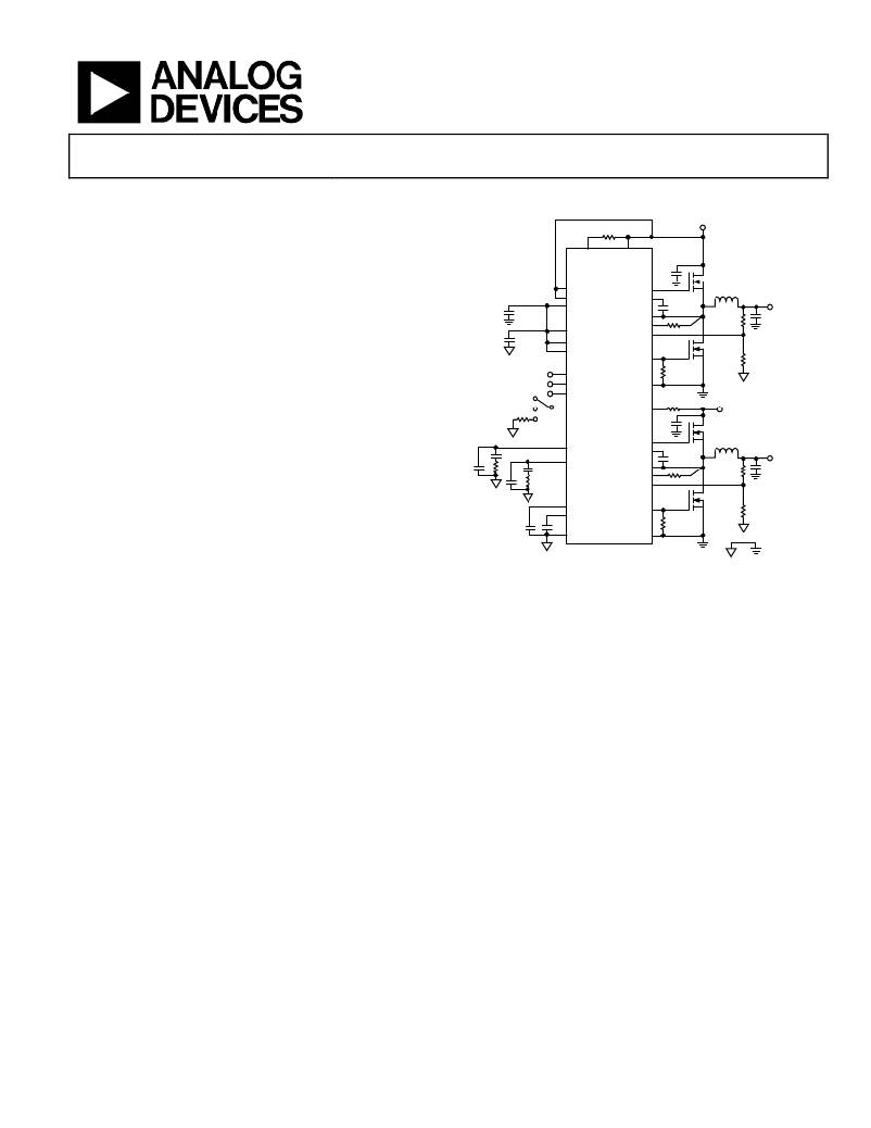
��TYPICAL� OPERATION� CIRCUIT�
�Wide� range� input:� 2.75� V� to� 20� V�
�Power� stage� input� voltage:� 1� V� to� 20� V�
�R� RAMP1�
�V� IN�
�Output� voltage� range:� 0.6� V� up� to� 90%� V� IN�
�RAMP1�
�VIN�
�DH1�
�BST1�
�VCCO�
�Output� current� to� more� than� 25� A� per� channel�
�Accurate� current� sharing� between� channels� (interleaved)�
�Programmable� frequency:� 200� kHz� to� 1.5� MHz�
�180°� phase� shift� between� channels� for� reduced� input�
�capacitance�
�±� 0.85%� reference� voltage� accuracy� from� ?40°C� to� +85°C�
�ADP1850�
�EN1�
�EN2�
�VDL�
�SW1�
�ILIM1�
�FB1�
�TRK1�
�TRK2�
�DL1�
�M1�
�M2�
�L1�
�R11�
�R12�
�V� OUT1�
�Integrated� boost� diodes�
�Power� saving� mode� (PSM)� at� light� loads�
�Accurate� power� good� with� internal� pull-up� resistor�
�HI�
�LO�
�PGOOD1�
�PGOOD2�
�SYNC�
�FREQ�
�PGND1�
�RAMP2�
�R� CSG1�
�R� RAMP2�
�V� IN�
�Accurate� voltage� tracking� capability�
�Independent� channel� precision� enable�
�Overvoltage� and� overcurrent� limit� protection�
�Externally� programmable� soft� start,� slope� compensation� and�
�current� sense� gain�
�Synchronization� input�
�Thermal� overload� protection�
�Input� undervoltage� lockout� (UVLO)�
�COMP1�
�COMP2�
�SS1�
�SS2�
�AGND�
�DH2�
�BST2�
�SW2�
�ILIM2�
�FB2�
�DL2�
�PGND2�
�R� CSG2�
�M3�
�M4�
�L2�
�R21�
�R22�
�V� OUT2�
�Available� in� 32-lead� 5� mm� � 5� mm� LFCSP�
�APPLICATIONS�
�High� current� single� and� dual� output� intermediate� bus� and�
�point� of� load� converters� requiring� sequencing� and�
�tracking� capability,� including� converters� for:�
�Point-of-load� power� supplies�
�Telecom� base� station� and� networking�
�Consumer�
�Industrial� and� instrumentation�
�Healthcare� and� medical�
�GENERAL� DESCRIPTION�
�The� ADP1850� is� a� configurable� dual� output� or� two-phase,� single�
�output� dc-to-dc� synchronous� buck� controller� capable� of� running�
�from� commonly� used� 3.3� V� to� 12� V� (up� to� 20� V)� voltage� inputs.�
�The� device� operates� in� current� mode� for� improved� transient�
�response� and� uses� valley� current� sensing� for� enhanced� noise�
�immunity.�
�The� architecture� enables� accurate� current� sharing� between�
�interleaved� phases� for� high� current� outputs.�
�The� ADP1850� is� ideal� in� system� applications� requiring� multiple�
�output� voltages:� the� ADP1850� includes� a� synchronization� fea-�
�ture� to� eliminate� beat� frequencies� between� switching� devices;�
�provides� accurate� tracking� capability� between� supplies� and�
�includes� precision� enable� for� simple,� robust� sequencing.�
�Rev.� A�
�Information� furnished� by� Analog� Devices� is� believed� to� be� accurate� and� reliable.� However,� no�
�responsibility� is� assumed� by� Analog� Devices� for� its� use,� nor� for� any� infringements� of� patents� or� other�
�rights� of� third� parties� that� may� result� from� its� use.� Specifications� subject� to� change� without� notice.� No�
�license� is� granted� by� implication� or� otherwise� under� any� patent� or� patent� rights� of� Analog� Devices.�
�Trademarks� and� registered� trademarks� are� the� property� of� their� respective� owners.�
�Figure� 1.� Single� Phase� Circuit�
�The� ADP1850� provides� high� speed,� high� peak� current� drive�
�capability� with� dead-time� optimization� to� enable� energy�
�efficient� power� conversion.� For� low� load� operation,� the� device�
�can� be� configured� to� operate� in� power� saving� mode� (PSM)� by�
�skipping� pulses� and� reducing� switching� losses� to� improve� the�
�energy� efficiency� at� light� load� and� standby� conditions.�
�The� accurate� current� limit� (±6%)� allows� the� power� architect� to�
�design� within� a� narrower� range� of� tolerances� and� can� reduce�
�overall� converter� size� and� cost.�
�The� ADP1850� provides� a� configurable� architecture� capable�
�of� wide� range� input� operation� to� provide� the� designer� with�
�maximum� re-use� opportunities� and� improved� time� to� market.�
�Additional� flexibility� is� provided� by� external� programmability�
�of� loop� compensation,� soft� start,� frequency� setting,� power�
�saving� mode,� current� limit� and� current� sense� gain� can� all� be�
�programmed� using� external� components.�
�The� ADP1850� includes� a� high� level� of� integration� in� a� small� size�
�package.� The� start-up� linear� regulator� and� the� boot-strap� diode�
�for� the� high� side� drive� are� included.� Protection� features� include:�
�undervoltage� lock-out,� overvoltage,� overcurrent/short-circuit�
�and� over� temperature.� The� ADP1850� is� available� in� a� compact�
�32-lead� LFCSP� 5� mm� � 5� mm� thermally� enhanced� package.�
�One� Technology� Way,� P.O.� Box� 9106,� Norwood,� MA� 02062-9106,� U.S.A.�
�Tel:� 781.329.4700� www.analog.com�
�Fax:� 781.461.3113� ?2010-2012� Analog� Devices,� Inc.� All� rights� reserved.�
�相关PDF资料 |
PDF描述 |
|---|---|
| A9BBG-1308F | FLEX CABLE - AFF13G/AF13/AFF13G |
| LQH43CN2R2M03L | INDUCTOR 2.2UH 20% 900MA 1812 |
| RB-3.305D | CONV DC/DC 1W 3.3VIN +/-05VOUT |
| TH3D336K020E0600 | CAP TANT 33UF 20V 10% 2917 |
| IR3316STRRPBF | IC SWITCH HISIDE PROGR D2PAK |
相关代理商/技术参数 |
参数描述 |
|---|---|
| ADP1851ACPZ-R7 | 功能描述:电流型 PWM 控制器 w-range input Synch StepDown DC/DC Cntr RoHS:否 制造商:Texas Instruments 开关频率:27 KHz 上升时间: 下降时间: 工作电源电压:6 V to 15 V 工作电源电流:1.5 mA 输出端数量:1 最大工作温度:+ 105 C 安装风格:SMD/SMT 封装 / 箱体:TSSOP-14 |
| ADP1851-EVALZ | 功能描述:电源管理IC开发工具 Evaluation Board 1.8V 25A Output RoHS:否 制造商:Maxim Integrated 产品:Evaluation Kits 类型:Battery Management 工具用于评估:MAX17710GB 输入电压: 输出电压:1.8 V |
| ADP1853 | 制造商:AD 制造商全称:Analog Devices 功能描述:Synchronous, Step-Down DC-to-DC Controller |
| ADP1853ACPZ-R7 | 功能描述:DC/DC 开关控制器 Synch StepDown DC/DC Cntr w/Volt trking RoHS:否 制造商:Texas Instruments 输入电压:6 V to 100 V 开关频率: 输出电压:1.215 V to 80 V 输出电流:3.5 A 输出端数量:1 最大工作温度:+ 125 C 安装风格: 封装 / 箱体:CPAK |
| ADP1853-EVALZ | 功能描述:电源管理IC开发工具 Evaluation Board 3.3V 20A Output RoHS:否 制造商:Maxim Integrated 产品:Evaluation Kits 类型:Battery Management 工具用于评估:MAX17710GB 输入电压: 输出电压:1.8 V |
发布紧急采购,3分钟左右您将得到回复。