- 您现在的位置:买卖IC网 > PDF目录17412 > ADP2114-EVALZ (Analog Devices Inc)BOARD EVALUATION 3.3V/1.8V PDF资料下载
参数资料
| 型号: | ADP2114-EVALZ |
| 厂商: | Analog Devices Inc |
| 文件页数: | 24/40页 |
| 文件大小: | 0K |
| 描述: | BOARD EVALUATION 3.3V/1.8V |
| 设计资源: | Powering AD9268 with ADP2114 for Increased Efficiency (CN0137) |
| 标准包装: | 1 |
| 主要目的: | DC/DC,步降 |
| 输出及类型: | 2,非隔离 |
| 输出电压: | 可调 |
| 电流 - 输出: | 4A,2A |
| 输入电压: | 2.75 ~ 5.5 V |
| 稳压器拓扑结构: | 降压 |
| 频率 - 开关: | 300kHz,600kHz,1.2MHz |
| 板类型: | 完全填充 |
| 已供物品: | 板 |
| 已用 IC / 零件: | ADP2114 |
第1页第2页第3页第4页第5页第6页第7页第8页第9页第10页第11页第12页第13页第14页第15页第16页第17页第18页第19页第20页第21页第22页第23页当前第24页第25页第26页第27页第28页第29页第30页第31页第32页第33页第34页第35页第36页第37页第38页第39页第40页
�� ��
��
��ADP2114�
�CONVERTER� CONFIGURATION�
�Data� Sheet�
�SELECTING� THE� OUTPUT� VOLTAGE�
�To� set� the� output� voltage,� V� OUT1� (V� OUT2� ),� select� one� of� the� six�
�fixed� voltages,� as� shown� in� Table� 4,� by� connecting� the� V1SET�
�(V2SET)� pin� to� GND� through� an� appropriate� value� resistor� (see�
��Channel� 1� and� Channel� 2,� respectively.� The� feedback� pin� FB1�
�To� limit� output� voltage� accuracy� degradation� due� to� FB� bias�
�current� to� less� than� 0.05%� (0.5%� maximum),� ensure� that� the�
�divider� string� current� is� greater� than� 20� μA.� To� calculate� the�
�desired� resistor� values,� first� determine� the� value� of� the� bottom�
�divider� string� resistor,� R1,� by�
�R1� =� V� REF� /� I� STRING�
�(2)�
�(3)�
�?� V� ?� V� REF� ?�
�(FB2)� should� be� directly� connected� to� V� OUT1� (V� OUT2� ).�
�Table� 4.� Output� Voltage� Programming�
�R� V1SET� (?)� ±� 5%� V� OUT1� (V)� R� V2SET� (?)� ±� 5%� V� OUT2� (V)�
�0� to� GND� 0.8� 0� to� GND� 0.8�
�4.7� k� to� GND� 1.2� 4.7� k� to� GND� 1.2�
�8.2� k� to� GND� 1.5� 8.2� k� to� GND� 1.5�
�15� k� to� GND� 1.8� 15� k� to� GND� 1.8�
�where:�
�V� REF� is� 0.6� V,� the� internal� reference.�
�I� STRING� is� the� resistor� divider� string� current.�
�When� R1� is� determined,� calculate� the� value� of� the� top� resistor,�
�R2,� by�
�R2� =� R1� ?� OUT� ?�
�?� V� REF� ?�
�27� k� to� GND�
�47� k� to� GND�
�2.5�
�3.3�
�27� k� to� GND�
�47� k� to� GND�
�2.5�
�3.3�
�R� FREQ�
�V� IN�
�82� k� to� GND�
�0� to� VDD�
�0.6� to� <1.6�
�(adjustable)�
�1.6� to� 3.3�
�(adjustable)�
�82� k� to� GND�
�0� to� VDD�
�0.6� to� <1.6�
�(adjustable)�
�1.6� to� 3.3�
�(adjustable)�
�V1SET/�
�V2SET�
�VINx�
�ADP2114�
�R� V1SET� /�
�R� V2SET�
�V� OUT1� /V� OUT2�
�If� the� required� output� voltage� V� OUT1� (V� OUT2� )� is� in� the� adjustable�
�range,� from� 0.6� V� to� less� than� 1.6� V,� connect� V1SET� (V2SET)�
�through� an� 82� k?� resistor� to� GND.� For� the� adjustable� output�
�voltage� range� of� 1.6� V� to� 3.3� V,� tie� V1SET� (V2SET)� to� VDD� (see�
�GND�
�SWx�
�FB1/FB2�
�PGNDx�
�COMP1/�
�COMP2�
�L�
��set� by� a� resistive� voltage� divider� from� the� output� voltage� to� the�
�feedback� pin� (see� Figure� 71).� The� ratio� of� the� resistive� voltage�
�divider� sets� the� output� voltage,� while� the� absolute� value� of� those�
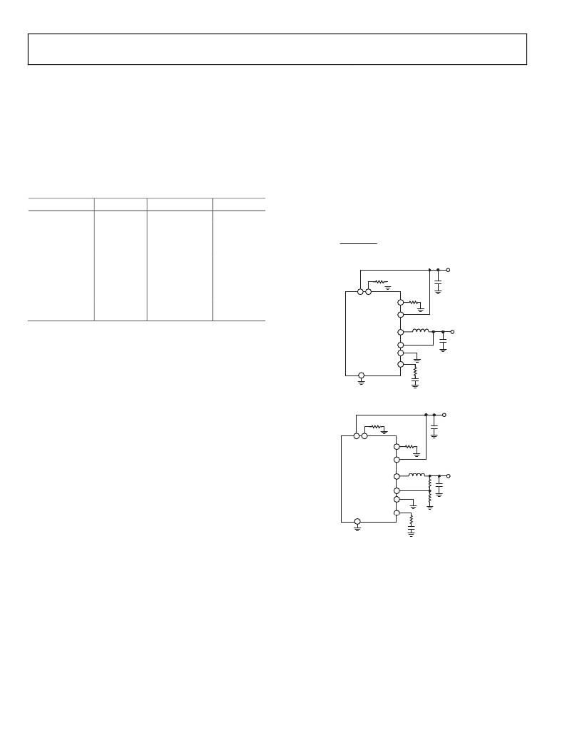
�Figure� 70.� Configuration� for� Fixed� Outputs�
�V� IN�
�R� FREQ�
�resistors� sets� the� divider� string� current.� For� lower� divider� string�
�currents,� the� small� 10� nA� (0.1� μA� maximum)� FB� bias� current�
�should� be� taken� into� account� when� calculating� the� resistor�
�values.� The� FB� bias� current� can� be� ignored� for� a� higher� divider�
�string� current;� however,� this� degrades� efficiency� at� very� light� loads.�
�V1SET/�
�V2SET�
�VINx�
�ADP2114�
�SWx�
�R� V1SET� /�
�R� V2SET�
�L�
�V� OUT1� /V� OUT2�
�R2�
�FB1/FB2�
�PGNDx�
�R1�
�GND�
�COMP1/�
�COMP2�
�Figure� 71.� Configuration� for� Adjustable� Outputs�
�Rev.� B� |� Page� 24� of� 40�
�相关PDF资料 |
PDF描述 |
|---|---|
| RCM12DCBI-S189 | CONN EDGECARD 24POS R/A .156 SLD |
| GCC28DCAD | CONN EDGECARD 56POS R/A .100 SLD |
| EL7232CN | IC LINE DRIVER DUAL 3ST 8-DIP |
| RCM12DCCI-S189 | CONN EDGECARD 24POS R/A .156 SLD |
| LM4040D20QDBZR | IC VREF SHUNT PREC 2.048V SOT23 |
相关代理商/技术参数 |
参数描述 |
|---|---|
| ADP2114-EVALZ | 制造商:Analog Devices 功能描述:4A Step-Down DC/DC Converter Evaluation 制造商:Analog Devices 功能描述:ADP2114, DC TO DC CONVERTER, STEP DOWN, EVAL BOARD |
| ADP2116 | 制造商:AD 制造商全称:Analog Devices 功能描述:Configurable, Dual 3 A/Single 6 A, Synchronous, Step-Down DC-to-DC Regulator |
| ADP2116ACPZ-R7 | 功能描述:IC REG BUCK SYNC ADJ 32LFCSP RoHS:是 类别:集成电路 (IC) >> PMIC - 稳压器 - DC DC 开关稳压器 系列:- 标准包装:2,500 系列:- 类型:降压(降压) 输出类型:固定 输出数:1 输出电压:1.2V,1.5V,1.8V,2.5V 输入电压:2.7 V ~ 20 V PWM 型:- 频率 - 开关:- 电流 - 输出:50mA 同步整流器:是 工作温度:-40°C ~ 125°C 安装类型:表面贴装 封装/外壳:10-TFSOP,10-MSOP(0.118",3.00mm 宽)裸露焊盘 包装:带卷 (TR) 供应商设备封装:10-MSOP 裸露焊盘 |
| ADP2116ACPZ-R7 | 制造商:Analog Devices 功能描述:DC/DC CONVERTER IC |
| ADP2116-BL1-EVZ | 功能描述:EVAL BOARD FOR ADP2116 RoHS:是 类别:编程器,开发系统 >> 评估板 - DC/DC 与 AC/DC(离线)SMPS 系列:- 标准包装:1 系列:- 主要目的:DC/DC,步降 输出及类型:1,非隔离 功率 - 输出:- 输出电压:3.3V 电流 - 输出:3A 输入电压:4.5 V ~ 28 V 稳压器拓扑结构:降压 频率 - 开关:250kHz 板类型:完全填充 已供物品:板 已用 IC / 零件:L7981 其它名称:497-12113STEVAL-ISA094V1-ND |
发布紧急采购,3分钟左右您将得到回复。