- 您现在的位置:买卖IC网 > PDF目录17412 > ADP2114-EVALZ (Analog Devices Inc)BOARD EVALUATION 3.3V/1.8V PDF资料下载
参数资料
| 型号: | ADP2114-EVALZ |
| 厂商: | Analog Devices Inc |
| 文件页数: | 25/40页 |
| 文件大小: | 0K |
| 描述: | BOARD EVALUATION 3.3V/1.8V |
| 设计资源: | Powering AD9268 with ADP2114 for Increased Efficiency (CN0137) |
| 标准包装: | 1 |
| 主要目的: | DC/DC,步降 |
| 输出及类型: | 2,非隔离 |
| 输出电压: | 可调 |
| 电流 - 输出: | 4A,2A |
| 输入电压: | 2.75 ~ 5.5 V |
| 稳压器拓扑结构: | 降压 |
| 频率 - 开关: | 300kHz,600kHz,1.2MHz |
| 板类型: | 完全填充 |
| 已供物品: | 板 |
| 已用 IC / 零件: | ADP2114 |
第1页第2页第3页第4页第5页第6页第7页第8页第9页第10页第11页第12页第13页第14页第15页第16页第17页第18页第19页第20页第21页第22页第23页第24页当前第25页第26页第27页第28页第29页第30页第31页第32页第33页第34页第35页第36页第37页第38页第39页第40页
�� �
�
�Data� Sheet�
�SETTING� THE� OSCILLATOR� FREQUENCY�
�The� ADP2114� channels� can� be� set� to� operate� in� one� of� the� three�
�preset� switching� frequencies:� 300� kHz,� 600� kHz,� or� 1.2� MHz.�
�For� 300� kHz� operation,� connect� the� FREQ� pin� to� GND.� For�
�600� kHz� or� 1.2� MHz� operation,� connect� a� resistor� between� the�
��ADP2114�
�An� external� clock� can� be� applied� to� the� SYNC/CLKOUT� pin�
�when� configured� as� an� input� to� synchronize� multiple� ADP2114s�
�to� the� same� external� clock.� The� f� SYNC� range� is� 400� kHz� to� 4� MHz,�
��for� an� illustration.�
�V� IN�
�Table� 5.� Oscillator� Frequency� Setting�
�27k?�
�27k?�
�R� FREQ� (?)� ±� 5%�
�f� SW� (kHz)�
�SCFG�
�FREQ�
�VDD�
�SCFG�
�FREQ�
�VDD�
�0� to� GND�
�8.2� k� to� GND�
�300�
�600�
�SYNC�
�(� f� SW� =� f� SYNC� /2)�
�SYNC�
�(� f� SW� =� f� SYNC� /2)�
�27� k� to� GND�
�1200�
�f� SYNC�
�ADP2114�
�ADP2114�
�Choice� of� the� switching� frequency� depends� on� the� required�
�dc-to-dc� conversion� ratio� and� is� limited� by� the� minimum� and�
�maximum� controllable� duty� cycle� shown� on� Figure� 72.� This� is�
�due� to� the� requirement� of� minimum� on� and� minimum� off� times�
�for� current� sensing� and� robust� operation.� The� choice� of�
�switching� frequency� is� also� determined� by� the� need� for� small�
�external� components.� For� small,� area� limited� power� solutions,�
�use� of� higher� switching� frequencies� is� recommended.�
�100�
�EXTERNAL� CLOCK� (2.4MHz)� TO� OTHER� ADP2114�
�Figure� 73.� Synchronization� with� External� Clock� (f� SW� =� 1.2� MHz� in� This� Case)�
�When� synchronizing� to� an� external� clock,� the� switching�
�frequency� f� SW� must� be� set� close� to� half� of� the� expected� external�
�clock� frequency� by� appropriately� terminating� the� FREQ� pin� as�
��V� IN�
�8.2k?� 8.2k?�
�90�
�SCFG�
�FREQ�
�VDD�
�SCFG�
�FREQ�
�VDD�
�80�
�70�
�SYNC�
�(� f� SW� =� f� SYNC� /2)�
�ADP2114�
�CLKOUT�
�(� f� SW� =� 2� � f� SW� )�
�ADP2114�
�60�
�50�
�40�
�30�
�20�
�10�
�MAXIMUM� LIMIT�
�MINIMUM� LIMIT;� V� IN� =� 2.75V�
�MINIMUM� LIMIT;� V� IN� =� 3.3V�
�MINIMUM� LIMIT;� V� IN� =� 5.5V�
�f� SYNC� =� 2� � f� SW�
�TO� OTHER� ADP2114�
�NOTES�
�1.� f� SW� =� 600kHz� SET� FOR� BOTH� ADP2114.�
�Figure� 74.� ADP2114� to� SYNC� with� Another� ADP2114�
�(Note� that� the� SCFG� of� the� master� is� tied� to� VDD.)�
�The� ADP2114� can� also� be� configured� to� output� a� clock� signal�
�0�
�200�
�400�
�600� 800�
�SWITCHING� FREQUENCY� (kHz)�
�1000�
�1200�
�on� the� SYNC/CLKOUT� pin� to� synchronize� multiple� ADP2114s�
�to� it� (see� Figure� 74).� The� CLKOUT� signal� is� 90o� phase� shifted� to�
�Figure� 72.� Duty� Cycle� Working� Limits�
�For� single� output,� multiphase� applications� that� operate� at� close�
�to� 50%� duty� cycle,� it� is� recommended� to� use� the� 1.2� MHz�
�switching� frequency� to� minimize� crosstalk� between� the� phases.�
�SYNCHRONIZATION� AND� CLKOUT�
�The� ADP2114� can� be� configured� to� output� an� internal� clock� or�
�synchronize� to� an� external� clock� at� the� STNC/CLKOUT� pin.�
�The� SYNC/CLKOUT� pin� is� a� bidirectional� pin� configured� by�
��Table� 6.� SYNC/CLKOUT� Configuration� Setting�
�the� internal� clock� of� the� channels� so� that� the� master� ADP2114�
�and� the� slave� channels� are� out� of� phase� (see� Figure� 75� for�
�additional� information).�
�CHANNEL 1 SW�
�4�
�CHANNEL 2 SW�
�3�
�SCFG�
�SYNC/CLKOUT�
�GND�
�VDD�
�Input�
�Output�
�1�
�INTERNAL CLKOUT�
�The� converter� switching� frequency,� f� SW� ,� is� half� of� the� synchroni-�
�zation� frequency� f� SYNC� /f� CLKOUT� as� shown� in� Equation� 4,� irrespective�
�of� whether� SYNC/CLKOUT� is� configured� as� an� input� or� output.�
�f� SYNC/� f� CLKOUT� =� 2� � f� SW�
�(4)�
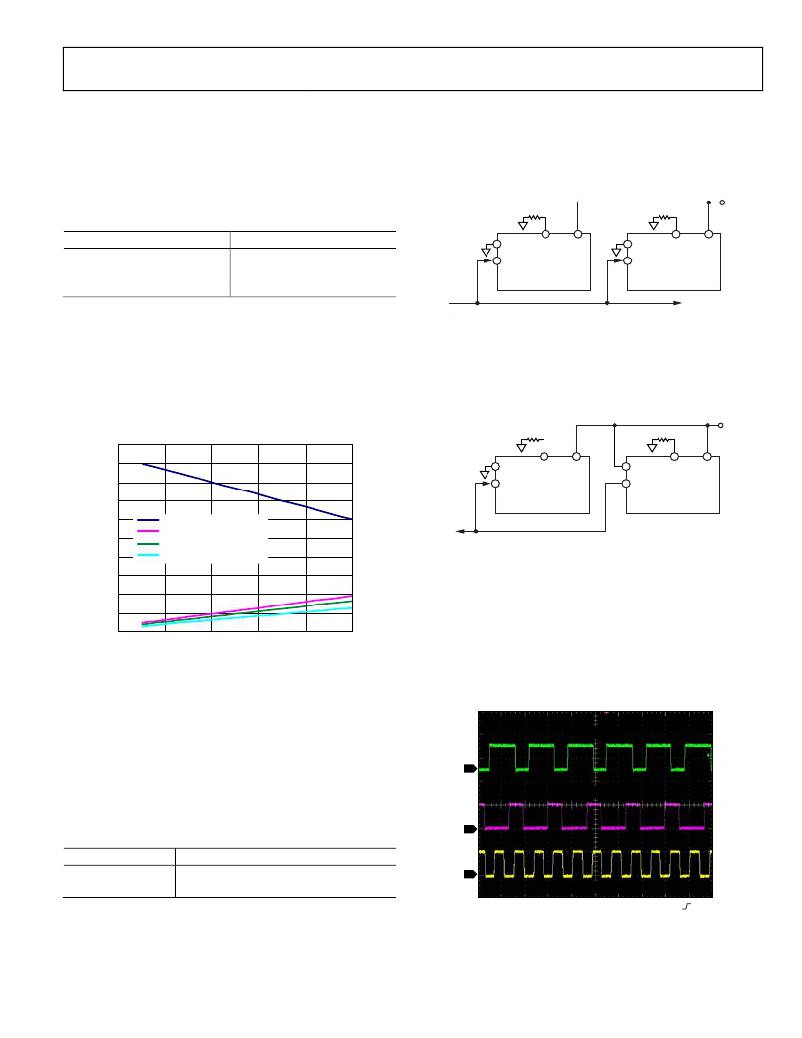
�CH1� 5.0V�
�CH3� 5.0V�
�M1.0μs� A� CH4�
�CH4� 5.0V�
�Figure� 75.� CLKOUT� Waveforms�
�3.00V�
�Rev.� B� |� Page� 25� of� 40�
�相关PDF资料 |
PDF描述 |
|---|---|
| RCM12DCBI-S189 | CONN EDGECARD 24POS R/A .156 SLD |
| GCC28DCAD | CONN EDGECARD 56POS R/A .100 SLD |
| EL7232CN | IC LINE DRIVER DUAL 3ST 8-DIP |
| RCM12DCCI-S189 | CONN EDGECARD 24POS R/A .156 SLD |
| LM4040D20QDBZR | IC VREF SHUNT PREC 2.048V SOT23 |
相关代理商/技术参数 |
参数描述 |
|---|---|
| ADP2114-EVALZ | 制造商:Analog Devices 功能描述:4A Step-Down DC/DC Converter Evaluation 制造商:Analog Devices 功能描述:ADP2114, DC TO DC CONVERTER, STEP DOWN, EVAL BOARD |
| ADP2116 | 制造商:AD 制造商全称:Analog Devices 功能描述:Configurable, Dual 3 A/Single 6 A, Synchronous, Step-Down DC-to-DC Regulator |
| ADP2116ACPZ-R7 | 功能描述:IC REG BUCK SYNC ADJ 32LFCSP RoHS:是 类别:集成电路 (IC) >> PMIC - 稳压器 - DC DC 开关稳压器 系列:- 标准包装:2,500 系列:- 类型:降压(降压) 输出类型:固定 输出数:1 输出电压:1.2V,1.5V,1.8V,2.5V 输入电压:2.7 V ~ 20 V PWM 型:- 频率 - 开关:- 电流 - 输出:50mA 同步整流器:是 工作温度:-40°C ~ 125°C 安装类型:表面贴装 封装/外壳:10-TFSOP,10-MSOP(0.118",3.00mm 宽)裸露焊盘 包装:带卷 (TR) 供应商设备封装:10-MSOP 裸露焊盘 |
| ADP2116ACPZ-R7 | 制造商:Analog Devices 功能描述:DC/DC CONVERTER IC |
| ADP2116-BL1-EVZ | 功能描述:EVAL BOARD FOR ADP2116 RoHS:是 类别:编程器,开发系统 >> 评估板 - DC/DC 与 AC/DC(离线)SMPS 系列:- 标准包装:1 系列:- 主要目的:DC/DC,步降 输出及类型:1,非隔离 功率 - 输出:- 输出电压:3.3V 电流 - 输出:3A 输入电压:4.5 V ~ 28 V 稳压器拓扑结构:降压 频率 - 开关:250kHz 板类型:完全填充 已供物品:板 已用 IC / 零件:L7981 其它名称:497-12113STEVAL-ISA094V1-ND |
发布紧急采购,3分钟左右您将得到回复。