- 您现在的位置:买卖IC网 > PDF目录17412 > ADP2114-EVALZ (Analog Devices Inc)BOARD EVALUATION 3.3V/1.8V PDF资料下载
参数资料
| 型号: | ADP2114-EVALZ |
| 厂商: | Analog Devices Inc |
| 文件页数: | 6/40页 |
| 文件大小: | 0K |
| 描述: | BOARD EVALUATION 3.3V/1.8V |
| 设计资源: | Powering AD9268 with ADP2114 for Increased Efficiency (CN0137) |
| 标准包装: | 1 |
| 主要目的: | DC/DC,步降 |
| 输出及类型: | 2,非隔离 |
| 输出电压: | 可调 |
| 电流 - 输出: | 4A,2A |
| 输入电压: | 2.75 ~ 5.5 V |
| 稳压器拓扑结构: | 降压 |
| 频率 - 开关: | 300kHz,600kHz,1.2MHz |
| 板类型: | 完全填充 |
| 已供物品: | 板 |
| 已用 IC / 零件: | ADP2114 |
第1页第2页第3页第4页第5页当前第6页第7页第8页第9页第10页第11页第12页第13页第14页第15页第16页第17页第18页第19页第20页第21页第22页第23页第24页第25页第26页第27页第28页第29页第30页第31页第32页第33页第34页第35页第36页第37页第38页第39页第40页
�� ��
��
��ADP2114�
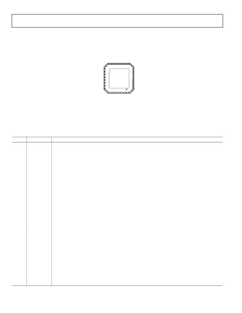
�PIN� CONFIGURATION� AND� FUNCTION� DESCRIPTIONS�
�Data� Sheet�
�GND�
�COMP1�
�1�
�2�
�24�
�23�
�SW1�
�SW2�
�FREQ�
�SCFG�
�SYNC/CLKOUT�
�OPCFG�
�COMP2�
�VDD�
�3�
�4�
�5�
�6�
�7�
�8�
�ADP2114�
�TOP� VIEW�
�(Not� to� Scale)�
�THERMAL� PAD�
�22�
�21�
�20�
�19�
�18�
�17�
�PGND1�
�PGND2�
�PGND3�
�PGND4�
�SW3�
�SW4�
�NOTES�
�1.� CONNECT� THE� EXPOSED� THERMAL� PAD� TO� THE�
�SIGNAL/ANALOG� GROUND� PLANE.�
�Figure� 3.� Pin� Configuration�
�Table� 3.� Pin� Function� Descriptions�
�Pin� No.�
�1�
�2�
�3�
�4�
�5�
�6�
�7�
�8�
�9�
�10�
�11�
�12�
�13�
�Mnemonic�
�GND�
�COMP1�
�FREQ�
�SCFG�
�SYNC/CLKOUT�
�OPCFG�
�COMP2�
�VDD�
�FB2�
�V2SET�
�SS2�
�PGOOD2�
�EN2�
�Description�
�Ground� for� the� Internal� Analog� and� Digital� Circuits.� Connect� GND� to� the� signal/analog� ground� plane� before�
�connecting� to� the� power� ground.�
�Error� Amplifier� Output� for� Channel� 1.� Connect� a� series� RC� network� from� COMP1� to� GND� to� compensate� for�
�Channel� 1.� For� multiphase� operation,� tie� COMP1� and� COMP2� together.�
�Frequency� Select� Input.� Connect� this� pin� through� a� resistor� to� GND� to� set� the� appropriate� switching� frequency�
��Synchronization� Configuration� Input.� SCFG� configures� the� SYNC/CLKOUT� pin� as� an� input� or� output.� Tie� this� pin�
�to� VDD� to� configure� SYNC/CLKOUT� as� an� output.� Tie� this� pin� to� GND� to� configure� SYNC/CLKOUT� as� an� input.�
�This� is� a� configurable� bidirectional� pin� (configured� with� the� SCFG� pin—see� the� Pin� 4� description� for� details).�
�When� SYNC/CLKOUT� is� an� output,� a� buffered� clock� of� twice� the� switching� frequency� with� a� phase� shift� of� 90°�
�is� available� on� this� pin.� When� configured� as� an� input,� this� pin� accepts� an� external� clock� to� which� the� converters�
�are� synchronized.� The� frequency� select� resistor,� mentioned� in� the� description� of� Pin� 3,� must� be� selected� close� to�
�the� expected� switching� frequency� for� stable� operation.�
�Operation� Configuration� Input.� Connect� this� pin� through� a� resistor� to� GND� to� set� the� system� mode� of� operation�
�according� to� Table� 7.� This� pin� can� be� used� to� select� a� peak� current� limit� for� each� power� channel� and� enable� or�
�disable� the� pulse� skip� mode.�
�Error� Amplifier� Output� for� Channel� 2.� Connect� a� series� RC� network� from� COMP2� to� GND� to� compensate� the�
�Channel� 2.� Tie� COMP1� and� COMP2� together� for� multiphase� configuration.�
�Power� Supply� Input.� The� power� source� for� the� ADP2114� internal� circuitry.� Connect� VDD� and� VINx� with� a�
�10� Ω� resistor� as� close� as� possible� to� the� ADP2114.� Bypass� VDD� to� GND� with� a� 1� μF� or� greater� capacitor.�
�Feedback� Voltage� Input� for� Channel� 2.� For� the� fixed� output� voltage� option,� connect� FB2� to� V� OUT2� .� For� the�
�adjustable� output� voltage� option,� connect� this� pin� to� a� resistor� divider� between� V� OUT2� and� GND.� The� reference�
�voltage� for� the� adjustable� output� voltage� option� is� 0.6� V.� With� multiphase� configurations,� connect� FB2� to� FB1�
�and� then� connect� them� to� V� OUT� .�
�Output� Voltage� Set� Pin� for� Channel� 2.� Connect� this� pin� through� a� resistor� to� GND� or� tie� to� VDD� to� select� a� fixed�
�output� voltage� option� (0.8� V,� 1.2� V,� 1.5� V,� 1.8� V,� 2.5� V,� or� 3.3� V)� or� an� adjust� output� voltage� for� V� OUT2� .� See� Table� 4�
�for� output� voltage� selection.�
�Soft� Start� Input� for� Channel� 2.� Place� a� capacitor� from� SS2� to� GND� to� set� the� soft� start� period.� A� 10� nF� capacitor�
�sets� a� 1� ms� soft� start� period.� For� multiphase� configuration,� connect� SS2� to� SS1.�
�Open-Drain� Power� Good� Output� for� Channel� 2.� Place� a� 100� kΩ� pull-up� resistor� to� VDD� or� any� other� voltage� ≤� 5.5� V;�
�PGOOD2� pulls� low� when� Channel� 2� is� out� of� regulation.�
�Enable� Input� for� Channel� 2.� Drive� EN2� high� to� turn� on� the� Channel� 2� converter� and� drive� EN2� low� to� turn� off�
�Channel� 2.� Tie� EN2� to� VDD� for� startup� with� VDD.� With� multiphase� configuration,� tie� EN2� to� EN1.�
�Rev.� B� |� Page� 6� of� 40�
�相关PDF资料 |
PDF描述 |
|---|---|
| RCM12DCBI-S189 | CONN EDGECARD 24POS R/A .156 SLD |
| GCC28DCAD | CONN EDGECARD 56POS R/A .100 SLD |
| EL7232CN | IC LINE DRIVER DUAL 3ST 8-DIP |
| RCM12DCCI-S189 | CONN EDGECARD 24POS R/A .156 SLD |
| LM4040D20QDBZR | IC VREF SHUNT PREC 2.048V SOT23 |
相关代理商/技术参数 |
参数描述 |
|---|---|
| ADP2114-EVALZ | 制造商:Analog Devices 功能描述:4A Step-Down DC/DC Converter Evaluation 制造商:Analog Devices 功能描述:ADP2114, DC TO DC CONVERTER, STEP DOWN, EVAL BOARD |
| ADP2116 | 制造商:AD 制造商全称:Analog Devices 功能描述:Configurable, Dual 3 A/Single 6 A, Synchronous, Step-Down DC-to-DC Regulator |
| ADP2116ACPZ-R7 | 功能描述:IC REG BUCK SYNC ADJ 32LFCSP RoHS:是 类别:集成电路 (IC) >> PMIC - 稳压器 - DC DC 开关稳压器 系列:- 标准包装:2,500 系列:- 类型:降压(降压) 输出类型:固定 输出数:1 输出电压:1.2V,1.5V,1.8V,2.5V 输入电压:2.7 V ~ 20 V PWM 型:- 频率 - 开关:- 电流 - 输出:50mA 同步整流器:是 工作温度:-40°C ~ 125°C 安装类型:表面贴装 封装/外壳:10-TFSOP,10-MSOP(0.118",3.00mm 宽)裸露焊盘 包装:带卷 (TR) 供应商设备封装:10-MSOP 裸露焊盘 |
| ADP2116ACPZ-R7 | 制造商:Analog Devices 功能描述:DC/DC CONVERTER IC |
| ADP2116-BL1-EVZ | 功能描述:EVAL BOARD FOR ADP2116 RoHS:是 类别:编程器,开发系统 >> 评估板 - DC/DC 与 AC/DC(离线)SMPS 系列:- 标准包装:1 系列:- 主要目的:DC/DC,步降 输出及类型:1,非隔离 功率 - 输出:- 输出电压:3.3V 电流 - 输出:3A 输入电压:4.5 V ~ 28 V 稳压器拓扑结构:降压 频率 - 开关:250kHz 板类型:完全填充 已供物品:板 已用 IC / 零件:L7981 其它名称:497-12113STEVAL-ISA094V1-ND |
发布紧急采购,3分钟左右您将得到回复。