- 您现在的位置:买卖IC网 > PDF目录14841 > ADP2164ACPZ-R7 (Analog Devices Inc)IC REG BUCK SYNC ADJ 4A 16LFCSP PDF资料下载
参数资料
| 型号: | ADP2164ACPZ-R7 |
| 厂商: | Analog Devices Inc |
| 文件页数: | 14/20页 |
| 文件大小: | 0K |
| 描述: | IC REG BUCK SYNC ADJ 4A 16LFCSP |
| 标准包装: | 1 |
| 类型: | 降压(降压) |
| 输出类型: | 可调式 |
| 输出数: | 1 |
| 输出电压: | 0.6 V ~ 6.5 V |
| 输入电压: | 2.7 V ~ 6.5 V |
| PWM 型: | 电流模式 |
| 频率 - 开关: | 500kHz ~ 1.4MHz |
| 电流 - 输出: | 4A |
| 同步整流器: | 是 |
| 工作温度: | -40°C ~ 125°C |
| 安装类型: | 表面贴装 |
| 封装/外壳: | 16-WQFN 裸露焊盘,CSP |
| 包装: | 标准包装 |
| 供应商设备封装: | 16-LFCSP-WQ(4x4) |
| 其它名称: | ADP2164ACPZ-R7DKR |
�� ��
��
��RT� (k� ?� )� =�
�ADP2164�
�THEORY� OF� OPERATION�
�The� ADP2164� is� a� step-down� dc-to-dc� regulator� that� uses�
�a� fixed-frequency,� peak� current� mode� architecture� with� an�
�integrated� high-side� switch� and� low-side� synchronous� rectifier.�
�The� high� switching� frequency� and� tiny,� 16-lead,� 4� mm� � 4� mm�
�LFCSP� package� provide� a� small,� step-down� dc-to-dc� regulator�
�solution.� The� integrated� high-side� switch� (P-channel� MOSFET)�
�and� synchronous� rectifier� (N-channel� MOSFET)� yield� high�
�efficiency.�
�The� ADP2164� operates� with� an� input� voltage� from� 2.7� V� to� 6.5� V�
�and� regulates� the� output� voltage� down� to� 0.6� V.� The� ADP2164� is�
�also� available� with� preset� output� voltage� options� of� 3.3� V,� 2.5� V,�
�1.8� V,� 1.5� V,� 1.2� V,� and� 1.0� V.�
�CONTROL� SCHEME�
�The� ADP2164� uses� a� fixed-frequency,� peak� current� mode�
�PWM� control� architecture.� At� the� start� of� each� oscillator� cycle,�
�the� P-channel� MOSFET� switch� is� turned� on,� placing� a� positive�
�voltage� across� the� inductor.� Current� in� the� inductor� increases�
�until� the� current� sense� signal� crosses� the� peak� inductor� current�
�level,� turns� off� the� P-channel� MOSFET� switch,� and� turns� on� the�
�N-channel� MOSFET� synchronous� rectifier.� This� action� places� a�
�negative� voltage� across� the� inductor,� causing� the� inductor� current�
�to� decrease.� The� synchronous� rectifier� stays� on� for� the� rest� of�
�the� cycle.�
�The� peak� inductor� current� level� is� set� by� the� compensation�
�(COMP)� voltage.� The� COMP� voltage� is� the� output� of� a� transcon-�
�ductance� error� amplifier� that� compares� the� feedback� voltage�
��SLOPE� COMPENSATION�
�To� prevent� subharmonic� oscillations,� slope� compensation�
�stabilizes� the� internal� current� control� loop� of� the� ADP2164�
�when� the� part� operates� at� or� beyond� a� 50%� duty� cycle.� Slope�
�compensation� is� implemented� by� summing� an� artificial� voltage�
�ramp� with� the� current� sense� signal� during� the� on� time� of� the�
�Data� Sheet�
�INTEGRATED� SOFT� START�
�The� ADP2164� has� integrated� soft� start� circuitry� to� limit� the�
�output� voltage� rise� time� and� reduce� inrush� current� at� startup.�
�The� soft� start� time� is� set� at� 2048� clock� cycles.�
�If� the� output� voltage� is� precharged� before� the� part� is� turned�
�on,� the� ADP2164� prevents� a� reverse� inductor� current—which�
�would� discharge� the� output� capacitor—until� the� soft� start�
�voltage� exceeds� the� voltage� on� the� FB� pin.�
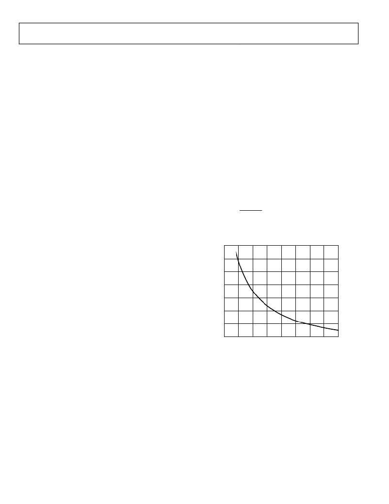
�OSCILLATOR� AND� SYNCHRONIZATION�
�The� ADP2164� switching� frequency� is� controlled� by� the� RT� pin.�
�If� the� RT� pin� is� connected� to� GND,� the� switching� frequency� is�
�set� to� 600� kHz.� If� the� RT� pin� is� connected� to� VIN,� the� switching�
�frequency� is� set� to� 1.2� MHz.�
�Connecting� a� resistor� from� RT� to� GND� allows� programming�
�of� the� switching� frequency� from� 500� kHz� to� 1.4� MHz.� Use� the�
�following� equation� to� set� the� switching� frequency:�
�54� ,� 000�
�f� S� (kHz)�
��frequency� and� the� RT� resistor.�
�1600�
�1400�
�1200�
�1000�
�800�
�600�
�400�
�P-channel� MOSFET� switch.� This� voltage� ramp� depends� on� the�
�output� voltage.� When� operating� at� high� output� voltages,� slope�
�200�
�20�
�40�
�60�
�80� 100� 120�
�RT� RESISTOR� (k?)�
�140�
�160�
�180�
�compensation� increases.� The� slope� compensation� ramp� value�
�determines� the� minimum� inductor� value� that� can� be� used� to�
�prevent� subharmonic� oscillations.�
�PRECISION� ENABLE/SHUTDOWN�
�The� EN� pin� is� a� precision� analog� input� that� enables� the� device�
�when� the� voltage� exceeds� 1.2� V� (typical);� this� pin� has� 100� mV�
�hysteresis.� When� the� enable� voltage� falls� below� 1.1� V� (typical),�
�the� part� turns� off.� To� force� the� ADP2164� to� start� automatically�
�when� input� power� is� applied,� connect� the� EN� pin� to� the� VIN� pin.�
�When� the� ADP2164� is� shut� down,� the� soft� start� capacitor� is�
�discharged.� This� causes� a� new� soft� start� cycle� to� begin� when�
�the� part� is� reenabled.�
�Figure� 37.� Switching� Frequency� vs.� RT� Resistor�
�To� synchronize� the� ADP2164� ,� drive� an� external� clock� at� the�
�SYNC� pin.� The� frequency� of� the� external� clock� can� be� in� the�
�range� of� 500� kHz� to� 1.4� MHz.�
�When� the� SYNC� pin� is� driven� by� an� external� clock,� the� user�
�can� configure� the� switching� frequency� to� be� in� phase� with� the�
�external� clock� or� 180°� out� of� phase� with� the� external� clock,� as�
�follows:�
�?� If� the� RT� pin� is� connected� to� GND� or� to� a� resistor,� the�
�switching� frequency� is� in� phase� with� the� external� clock.�
�?� If� the� RT� pin� is� connected� to� VIN,� the� switching� frequency�
�is� 180°� out� of� phase� with� the� external� clock.�
�An� internal� pull-down� resistor� (1� M?)� prevents� accidental�
�enabling� of� the� part� if� the� EN� input� is� left� floating.�
�Rev.� A� |� Page� 14� of� 20�
�相关PDF资料 |
PDF描述 |
|---|---|
| MAX6462XR49+T | IC VOLT DETECTOR LP SC70-3 |
| EBC26DRTI-S734 | CONN EDGECARD 52POS DIP .100 SLD |
| LTC3565EMSE#PBF | IC REG BUCK SYNC ADJ 10MSOP |
| ISC1812EB391J | INDUCTOR WW 390UH 5% 1812 |
| LT1610IS8#PBF | IC REG BOOST ADJ 0.6A 8SOIC |
相关代理商/技术参数 |
参数描述 |
|---|---|
| ADP2164-EVALZ | 功能描述:BOARD EVAL REG DC-DC 6.5V 4A RoHS:是 类别:编程器,开发系统 >> 评估板 - DC/DC 与 AC/DC(离线)SMPS 系列:- 标准包装:1 系列:- 主要目的:DC/DC,步降 输出及类型:1,非隔离 功率 - 输出:- 输出电压:3.3V 电流 - 输出:3A 输入电压:4.5 V ~ 28 V 稳压器拓扑结构:降压 频率 - 开关:250kHz 板类型:完全填充 已供物品:板 已用 IC / 零件:L7981 其它名称:497-12113STEVAL-ISA094V1-ND |
| ADP2165ACPZ-1.0-R7 | 功能描述:Buck Switching Regulator IC Positive Fixed 1V 1 Output 5A 24-WFQFN Exposed Pad, CSP 制造商:analog devices inc. 系列:- 包装:剪切带(CT) 零件状态:有效 功能:降压 输出配置:正 拓扑:降压 输出类型:固定 输出数:1 电压 - 输入(最小值):2.7V 电压 - 输入(最大值):5.5V 电压 - 输出(最小值/固定):1V 电压 - 输出(最大值):- 电流 - 输出:5A 频率 - 开关:250kHz ~ 1.4MHz 同步整流器:是 工作温度:-40°C ~ 125°C (TJ) 安装类型:表面贴装 封装/外壳:24-WFQFN 裸露焊盘,CSP 供应商器件封装:24-LFCSP-WQ(4x4) 标准包装:1 |
| ADP2165ACPZ-1.2-R7 | 功能描述:Buck Switching Regulator IC Positive Fixed 1.2V 1 Output 5A 24-WFQFN Exposed Pad, CSP 制造商:analog devices inc. 系列:- 包装:剪切带(CT) 零件状态:有效 功能:降压 输出配置:正 拓扑:降压 输出类型:固定 输出数:1 电压 - 输入(最小值):2.7V 电压 - 输入(最大值):5.5V 电压 - 输出(最小值/固定):1.2V 电压 - 输出(最大值):- 电流 - 输出:5A 频率 - 开关:250kHz ~ 1.4MHz 同步整流器:是 工作温度:-40°C ~ 125°C (TJ) 安装类型:表面贴装 封装/外壳:24-WFQFN 裸露焊盘,CSP 供应商器件封装:24-LFCSP-WQ(4x4) 标准包装:1 |
| ADP2165ACPZ-1.5-R7 | 功能描述:Buck Switching Regulator IC Positive Fixed 1.5V 1 Output 5A 24-WFQFN Exposed Pad, CSP 制造商:analog devices inc. 系列:- 包装:剪切带(CT) 零件状态:有效 功能:降压 输出配置:正 拓扑:降压 输出类型:固定 输出数:1 电压 - 输入(最小值):2.7V 电压 - 输入(最大值):5.5V 电压 - 输出(最小值/固定):1.5V 电压 - 输出(最大值):- 电流 - 输出:5A 频率 - 开关:250kHz ~ 1.4MHz 同步整流器:是 工作温度:-40°C ~ 125°C (TJ) 安装类型:表面贴装 封装/外壳:24-WFQFN 裸露焊盘,CSP 供应商器件封装:24-LFCSP-WQ(4x4) 标准包装:1 |
| ADP2165ACPZ-1.8-R7 | 功能描述:Buck Switching Regulator IC Positive Fixed 1.8V 1 Output 5A 24-WFQFN Exposed Pad, CSP 制造商:analog devices inc. 系列:- 包装:剪切带(CT) 零件状态:有效 功能:降压 输出配置:正 拓扑:降压 输出类型:固定 输出数:1 电压 - 输入(最小值):2.7V 电压 - 输入(最大值):5.5V 电压 - 输出(最小值/固定):1.8V 电压 - 输出(最大值):- 电流 - 输出:5A 频率 - 开关:250kHz ~ 1.4MHz 同步整流器:是 工作温度:-40°C ~ 125°C (TJ) 安装类型:表面贴装 封装/外壳:24-WFQFN 裸露焊盘,CSP 供应商器件封装:24-LFCSP-WQ(4x4) 标准包装:1 |
发布紧急采购,3分钟左右您将得到回复。