- 您现在的位置:买卖IC网 > PDF目录14841 > ADP2164ACPZ-R7 (Analog Devices Inc)IC REG BUCK SYNC ADJ 4A 16LFCSP PDF资料下载
参数资料
| 型号: | ADP2164ACPZ-R7 |
| 厂商: | Analog Devices Inc |
| 文件页数: | 16/20页 |
| 文件大小: | 0K |
| 描述: | IC REG BUCK SYNC ADJ 4A 16LFCSP |
| 标准包装: | 1 |
| 类型: | 降压(降压) |
| 输出类型: | 可调式 |
| 输出数: | 1 |
| 输出电压: | 0.6 V ~ 6.5 V |
| 输入电压: | 2.7 V ~ 6.5 V |
| PWM 型: | 电流模式 |
| 频率 - 开关: | 500kHz ~ 1.4MHz |
| 电流 - 输出: | 4A |
| 同步整流器: | 是 |
| 工作温度: | -40°C ~ 125°C |
| 安装类型: | 表面贴装 |
| 封装/外壳: | 16-WQFN 裸露焊盘,CSP |
| 包装: | 标准包装 |
| 供应商设备封装: | 16-LFCSP-WQ(4x4) |
| 其它名称: | ADP2164ACPZ-R7DKR |
�� ��
��
��ADP2164�
�Data� Sheet�
�APPLICATIONS� INFORMATION�
�ADISIMPOWER� DESIGN� TOOL�
�The� ADP2164� is� supported� by� ADIsimPower� design� tool� set.�
�L� =�
�(� V� IN� ?� V� OUT� )� � D�
�?� I� L� � f� S�
�10?�
�C1� C� IN� 3.3V�
�10k?�
�10V�
�L�
�V� OUT�
�ADP2164ACPZ� C� OUT1� C� OUT2�
�3�
�10�
�TRK�
�SW�
�6.3V�
�6.3V�
�I� PEAK� =� I� O� +�
�ADIsimPower� is� a� collection� of� tools� that� produce� complete�
�power� designs� optimized� for� a� specific� design� goal.� The� tools�
�enable� the� user� to� generate� a� full� schematic,� bill� of� materials,�
�and� calculate� performance� in� minutes.� ADIsimPower� can�
�optimize� designs� for� cost,� area,� efficiency,� and� parts� count�
�while� taking� into� consideration� the� operating� conditions� and�
�limitations� of� the� IC� and� all� real� external� components.� For�
�more� information� about� ADIsimPower� design� tools,� refer� to�
�www.analog.com/ADIsimPower� .� The� tool� set� is� available� from�
�this� website,� and� users� can� also� request� an� unpopulated� board�
�through� the� tool.�
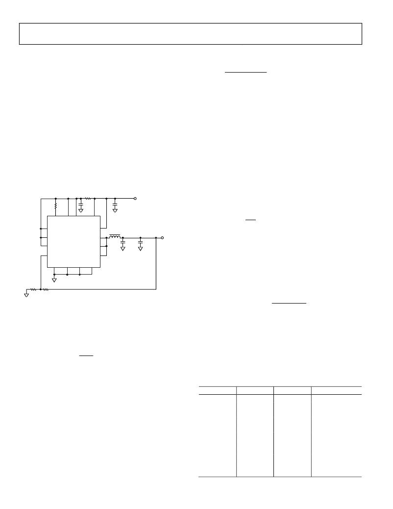
�The� typical� application� circuit� for� the� ADP2164� is� shown� in�
��R1�
�V� IN�
�R2�
�0.1μF� 47μF�
�X5R�
�16� 15� 14� 13�
�PGOOD� EN� VIN� PVIN�
�1� 12�
�SYNC� PVIN�
�0.8μH�
�2� 11�
�RT� SW� 1.2V�
�4A�
�47μF� 100μF�
�X5R� X5R�
�4� 9�
�FB� SW�
�GND� PGND� PGND� PGND�
�where:�
�V� IN� is� the� input� voltage.�
�V� OUT� is� the� output� voltage.�
�ΔI� L� is� the� inductor� current� ripple.�
�f� S� is� the� switching� frequency.�
�D� is� the� duty� cycle� (V� OUT� /V� IN� ).�
�The� ADP2164� uses� slope� compensation� in� the� current� control�
�loop� to� prevent� subharmonic� oscillations� when� the� duty� cycle�
�is� larger� than� 50%.� The� internal� slope� compensation� limits� the�
�minimum� inductor� value.�
�The� negative� current� limit� (?1.3� A)� also� limits� the� minimum�
�inductor� value.� The� inductor� current� ripple� (ΔI� L� )� calculated� by�
�the� selected� inductor� should� not� exceed� 2.6� A.�
�The� peak� inductor� current� should� be� kept� below� the� peak� current�
�limit� threshold� and� is� calculated� using� the� following� equation:�
�?� I� L�
�2�
�Ensure� that� the� rms� current� of� the� selected� inductor� is� greater�
�than� the� maximum� load� current� and� that� its� saturation� current�
�is� greater� than� the� peak� current� limit� of� the� converter.�
�OUTPUT� CAPACITOR� SELECTION�
�R� BOT�
�10k?�
�R� TOP�
�10k?�
�5�
�6�
�7�
�8�
�L:� MSS1048-801NL� COILCRAFT�
�C� IN� :� C3225X5R1A476M� TDK�
�C� OUT1� :� C3225X5R0J476M� TDK�
�C� OUT2� :� C3225X5R0J107M� TDK�
�The� output� capacitor� value� is� determined� by� the� output� voltage�
�ripple,� load� step� transient,� and� loop� stability.� The� output� ripple�
�is� determined� by� the� ESR� and� the� capacitance.�
�R� TOP�
�?�
�V� OUT� =� 0� .� 6� � ?� ?� 1� +�
�R� BOT�
�?�
�?�
�1�
�?� V� OUT� =� ?� I� L� � ?� ESR� +�
�?�
�8� � C� OUT� � f� S� ?� ?�
�?�
�Figure� 38.� Typical� Application� Circuit�
�OUTPUT� VOLTAGE� SELECTION�
�The� output� voltage� of� the� adjustable� version� of� the� ADP2164� is�
�set� by� an� external� resistive� voltage� divider� using� the� following�
�equation:�
�?� ?�
�?�
�To� limit� output� voltage� accuracy� degradation� due� to� FB� bias�
�current� (0.1� μA� maximum)� to� less� than� 0.5%� (maximum),�
�ensure� that� R� BOT� is� less� than� 30� k?.�
�?� ?�
�?�
�The� load� step� transient� response� depends� on� the� inductor,� the�
�output� capacitor,� and� the� current� control� loop.�
�The� ADP2164� has� integrated� loop� compensation� for� simple�
�power� design.� Table� 5� and� Table� 6� show� the� recommended�
�values� for� inductors� and� capacitors� for� the� ADP2164� based�
�on� the� input� and� output� voltages� for� the� part.� X5R� or� X7R�
�dielectric� ceramic� capacitors� are� highly� recommended.�
�Table� 5.� Recommended� L� and� C� OUT� Values� at� f� S� =� 1.2� MHz�
�V� IN� (V)� V� OUT� (V)� L� (μH� )� C� OUT� (μF)�
�INDUCTOR� SELECTION�
�The� inductor� value� is� determined� by� the� operating� frequency,�
�input� voltage,� output� voltage,� and� ripple� current.� A� small� inductor�
�value� provides� larger� inductor� current� ripple� and� fast� transient�
�response� but� degrades� efficiency;� a� large� inductor� value� provides�
�small� inductor� current� ripple� and� good� efficiency� but� slows�
�transient� response.� For� a� reasonable� trade-off� between� transient�
�response� and� efficiency,� the� inductor� current� ripple,� ΔI� L� ,� is� typically�
�set� to� one-third� the� maximum� load� current.� The� inductor� value�
�is� calculated� using� the� following� equation:�
�3.3�
�3.3�
�3.3�
�3.3�
�3.3�
�5�
�5�
�5�
�5�
�5�
�5�
�1.0�
�1.2�
�1.5�
�1.8�
�2.5�
�1.0�
�1.2�
�1.5�
�1.8�
�2.5�
�3.3�
�0.8�
�0.8�
�1�
�1�
�1�
�0.8�
�0.8�
�1�
�1�
�1�
�1�
�100� +� 100�
�100� +� 47�
�100� +� 47�
�100�
�47�
�100� +� 100�
�100� +� 47�
�100� +� 47�
�100�
�47�
�47�
�Rev.� A� |� Page� 16� of� 20�
�相关PDF资料 |
PDF描述 |
|---|---|
| MAX6462XR49+T | IC VOLT DETECTOR LP SC70-3 |
| EBC26DRTI-S734 | CONN EDGECARD 52POS DIP .100 SLD |
| LTC3565EMSE#PBF | IC REG BUCK SYNC ADJ 10MSOP |
| ISC1812EB391J | INDUCTOR WW 390UH 5% 1812 |
| LT1610IS8#PBF | IC REG BOOST ADJ 0.6A 8SOIC |
相关代理商/技术参数 |
参数描述 |
|---|---|
| ADP2164-EVALZ | 功能描述:BOARD EVAL REG DC-DC 6.5V 4A RoHS:是 类别:编程器,开发系统 >> 评估板 - DC/DC 与 AC/DC(离线)SMPS 系列:- 标准包装:1 系列:- 主要目的:DC/DC,步降 输出及类型:1,非隔离 功率 - 输出:- 输出电压:3.3V 电流 - 输出:3A 输入电压:4.5 V ~ 28 V 稳压器拓扑结构:降压 频率 - 开关:250kHz 板类型:完全填充 已供物品:板 已用 IC / 零件:L7981 其它名称:497-12113STEVAL-ISA094V1-ND |
| ADP2165ACPZ-1.0-R7 | 功能描述:Buck Switching Regulator IC Positive Fixed 1V 1 Output 5A 24-WFQFN Exposed Pad, CSP 制造商:analog devices inc. 系列:- 包装:剪切带(CT) 零件状态:有效 功能:降压 输出配置:正 拓扑:降压 输出类型:固定 输出数:1 电压 - 输入(最小值):2.7V 电压 - 输入(最大值):5.5V 电压 - 输出(最小值/固定):1V 电压 - 输出(最大值):- 电流 - 输出:5A 频率 - 开关:250kHz ~ 1.4MHz 同步整流器:是 工作温度:-40°C ~ 125°C (TJ) 安装类型:表面贴装 封装/外壳:24-WFQFN 裸露焊盘,CSP 供应商器件封装:24-LFCSP-WQ(4x4) 标准包装:1 |
| ADP2165ACPZ-1.2-R7 | 功能描述:Buck Switching Regulator IC Positive Fixed 1.2V 1 Output 5A 24-WFQFN Exposed Pad, CSP 制造商:analog devices inc. 系列:- 包装:剪切带(CT) 零件状态:有效 功能:降压 输出配置:正 拓扑:降压 输出类型:固定 输出数:1 电压 - 输入(最小值):2.7V 电压 - 输入(最大值):5.5V 电压 - 输出(最小值/固定):1.2V 电压 - 输出(最大值):- 电流 - 输出:5A 频率 - 开关:250kHz ~ 1.4MHz 同步整流器:是 工作温度:-40°C ~ 125°C (TJ) 安装类型:表面贴装 封装/外壳:24-WFQFN 裸露焊盘,CSP 供应商器件封装:24-LFCSP-WQ(4x4) 标准包装:1 |
| ADP2165ACPZ-1.5-R7 | 功能描述:Buck Switching Regulator IC Positive Fixed 1.5V 1 Output 5A 24-WFQFN Exposed Pad, CSP 制造商:analog devices inc. 系列:- 包装:剪切带(CT) 零件状态:有效 功能:降压 输出配置:正 拓扑:降压 输出类型:固定 输出数:1 电压 - 输入(最小值):2.7V 电压 - 输入(最大值):5.5V 电压 - 输出(最小值/固定):1.5V 电压 - 输出(最大值):- 电流 - 输出:5A 频率 - 开关:250kHz ~ 1.4MHz 同步整流器:是 工作温度:-40°C ~ 125°C (TJ) 安装类型:表面贴装 封装/外壳:24-WFQFN 裸露焊盘,CSP 供应商器件封装:24-LFCSP-WQ(4x4) 标准包装:1 |
| ADP2165ACPZ-1.8-R7 | 功能描述:Buck Switching Regulator IC Positive Fixed 1.8V 1 Output 5A 24-WFQFN Exposed Pad, CSP 制造商:analog devices inc. 系列:- 包装:剪切带(CT) 零件状态:有效 功能:降压 输出配置:正 拓扑:降压 输出类型:固定 输出数:1 电压 - 输入(最小值):2.7V 电压 - 输入(最大值):5.5V 电压 - 输出(最小值/固定):1.8V 电压 - 输出(最大值):- 电流 - 输出:5A 频率 - 开关:250kHz ~ 1.4MHz 同步整流器:是 工作温度:-40°C ~ 125°C (TJ) 安装类型:表面贴装 封装/外壳:24-WFQFN 裸露焊盘,CSP 供应商器件封装:24-LFCSP-WQ(4x4) 标准包装:1 |
发布紧急采购,3分钟左右您将得到回复。