- 您现在的位置:买卖IC网 > PDF目录20384 > ADP2301-EVALZ (Analog Devices Inc)BOARD EVALUATION FOR ADP2301 PDF资料下载
参数资料
| 型号: | ADP2301-EVALZ |
| 厂商: | Analog Devices Inc |
| 文件页数: | 16/28页 |
| 文件大小: | 0K |
| 描述: | BOARD EVALUATION FOR ADP2301 |
| 标准包装: | 1 |
| 主要目的: | DC/DC,步降 |
| 输出及类型: | 1,非隔离 |
| 输出电压: | 3.3V |
| 电流 - 输出: | 1.2A |
| 输入电压: | 3 ~ 20 V |
| 稳压器拓扑结构: | 降压 |
| 频率 - 开关: | 1.4MHz |
| 板类型: | 完全填充 |
| 已供物品: | 板 |
| 已用 IC / 零件: | ADP2301 |
第1页第2页第3页第4页第5页第6页第7页第8页第9页第10页第11页第12页第13页第14页第15页当前第16页第17页第18页第19页第20页第21页第22页第23页第24页第25页第26页第27页第28页
�� ��
��
��?�
�V� OUT� =� 0� .� 800� V� � ?� ?� 1� +� FB� 1�
�R� FB� 2�
�?�
�?�
�ADP2300/ADP2301�
�APPLICATIONS� INFORMATION�
�ADIsimPower� DESIGN� TOOL�
�The� ADP2300/ADP2301� are� supported� by� the� ADIsimPower�
�design� tool� set.� ADIsimPower� is� a� collection� of� tools� that� produce�
�complete� power� designs� optimized� for� a� specific� design� goal.�
�The� tools� enable� the� user� to� generate� a� full� schematic� and� bill� of�
�materials,� and� calculate� performance� in� minutes.� ADIsimPower�
�can� optimize� designs� for� cost,� area,� efficiency,� and� parts� count�
�while� taking� into� consideration� the� operating� conditions� and�
�limitations� of� the� IC� and� all� real� external� components.� For�
�more� information� about� ADIsimPower� design� tools,� refer� to�
�www.analog.com/ADIsimPower� .� The� tool� set� is� available� from�
�this� website,� and� users� can� request� an� unpopulated� board�
�through� the� tool.�
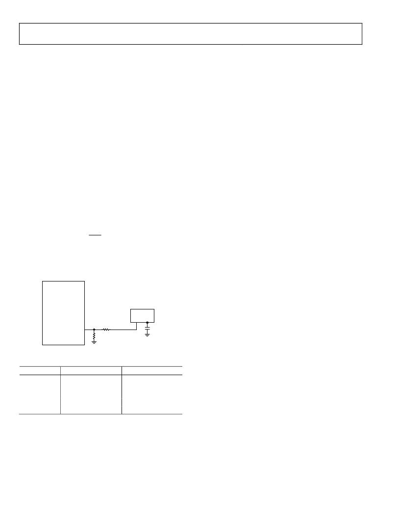
�PROGRAMMING� THE� OUTPUT� VOLTAGE�
�The� output� voltage� of� the� ADP2300/ADP2301� is� externally� set� by�
�a� resistive� voltage� divider� from� the� output� voltage� to� the� FB� pin,�
�as� shown� in� Figure� 42.� Suggested� resistor� values� for� the� typical�
�output� voltage� setting� are� listed� in� Table� 6.� The� equation� for� the�
�output� voltage� setting� is�
�?� R� ?�
�?�
�where:�
�V� OUT� is� the� output� voltage.�
�R� FB1� is� the� feedback� resistor� from� V� OUT� to� FB.�
�R� FB2� is� the� feedback� resistor� from� FB� to� GND.�
�Data� Sheet�
�VOLTAGE� CONVERSION� LIMITATIONS�
�There� are� both� lower� and� upper� output� voltage� limitations� for� a�
�given� input� voltage� due� to� the� minimum� on� time,� the� minimum�
�off� time,� and� the� bootstrap� dropout� voltage.�
�The� lower� limit� of� the� output� voltage� is� constrained� by� the� finite,�
�controllable� minimum� on� time,� which� can� be� as� high� as� 135� ns� for�
�the� worst� case.� By� considering� the� variation� of� both� the� switching�
�frequency� and� the� input� voltage,� the� equation� for� the� lower� limit�
�of� the� output� voltage� is�
�V� OUT� (min)� =� t� MIN� -� ON� � f� SW� (max)� � (� V� IN� (max)� +� V� D� )� ?� V� D�
�where:�
�V� IN(max)� is� the� maximum� input� voltage.�
�f� SW(max� )� is� the� maximum� switching� frequency� for� the� worst� case.�
�t� MIN-ON� is� the� minimum� controllable� on� time.�
�V� D� is� the� diode� forward� drop.�
�The� upper� limit� of� the� output� voltage� is� constrained� by� the� mini-�
�mum� controllable� off� time,� which� can� be� as� high� as� 120� ns� in�
�the� ADP2301� for� the� worst� case.� By� considering� the� variation� of�
�both� the� switching� frequency� and� the� input� voltage,� the� equation�
�for� the� upper� limit� of� the� output� voltage� is�
�V� OUT� (max)� =� (� 1� ?� t� MIN� -� OFF� � f� SW� (max)� )� � (� V� IN� (min)� +� V� D� )� ?� V� D�
�where:�
�V� IN(min)� is� the� minimum� input� voltage.�
�f� SW(max)� is� the� maximum� switching� frequency� for� the� worst� case.�
�V� D� is� the� diode� forward� drop.�
�t� MIN-OFF� is� the� minimum� controllable� off� time.�
�In� addition,� the� bootstrap� circuit� limits� the� minimum� input�
�ADP2300/�
�ADP2301�
�FB�
�R� FB1�
�R� FB2�
�V� OUT�
�voltage� for� the� desired� output� due� to� internal� dropout� voltage.�
�To� attain� stable� operation� at� light� loads� and� ensure� proper� startup�
�for� the� prebias� condition,� the� ADP2300/ADP2301� require� the�
�voltage� difference� between� the� input� voltage� and� the� regulated�
�output� voltage� (or� between� the� input� voltage� and� the� prebias�
�voltage)� to� be� greater� than� 2.1� V� for� the� worst� case.� If� the� voltage�
�Figure� 42.� Programming� the� Output� Voltage� Using� a� Resistive� Voltage� Divider�
�Table� 6.� Suggested� Values� for� Resistive� Voltage� Divider�
�V� OUT� (V)� R� FB1� (kΩ),� ±1%� R� FB2� (kΩ),� ±1%�
�1.2� 4.99� 10�
�difference� is� smaller,� the� bootstrap� circuit� relies� on� some� minimum�
��shows� the� typical� required� minimum� input� voltage� vs.� load� current�
�for� the� 3.3� V� output� voltage.�
�1.8�
�2.5�
�3.3�
�5.0�
�12.7�
�21.5�
�31.6�
�52.3�
�10.2�
�10.2�
�10.2�
�10�
�Rev.� C� |� Page� 16� of� 28�
�相关PDF资料 |
PDF描述 |
|---|---|
| IR2103STR | IC DRIVER HALF BRIDGE 600V 8SOIC |
| RCC18DCMI-S288 | CONN EDGECARD 36POS .100 EXTEND |
| EBM12DRYH-S13 | CONN EDGECARD 24POS .156 EXTEND |
| R1S-2405/EH | CONV DC/DC 1W 24VIN 05VOUT |
| VE-B6B-CW-F4 | CONVERTER MOD DC/DC 95V 100W |
相关代理商/技术参数 |
参数描述 |
|---|---|
| ADP2302 | 制造商:AD 制造商全称:Analog Devices 功能描述:Quad-Channel, 12-Bit, Serial Input, 4 mA to 20 mA |
| ADP2302_12 | 制造商:AD 制造商全称:Analog Devices 功能描述:2 A/3 A, 20 V, 700 kHz, Nonsynchronous Step-Down Regulators |
| ADP2302ARDZ | 功能描述:IC REG BUCK ADJ 2A 8SOIC RoHS:是 类别:集成电路 (IC) >> PMIC - 稳压器 - DC DC 开关稳压器 系列:- 标准包装:250 系列:- 类型:降压(降压) 输出类型:固定 输出数:1 输出电压:1.2V 输入电压:2.05 V ~ 6 V PWM 型:电压模式 频率 - 开关:2MHz 电流 - 输出:500mA 同步整流器:是 工作温度:-40°C ~ 85°C 安装类型:表面贴装 封装/外壳:6-UFDFN 包装:带卷 (TR) 供应商设备封装:6-SON(1.45x1) 产品目录页面:1032 (CN2011-ZH PDF) 其它名称:296-25628-2 |
| ADP2302ARDZ-2.5 | 制造商:Analog Devices 功能描述: |
| ADP2302ARDZ-2.5-R7 | 功能描述:IC REG BUCK 2.5V 2A 8SOIC RoHS:是 类别:集成电路 (IC) >> PMIC - 稳压器 - DC DC 开关稳压器 系列:- 标准包装:500 系列:- 类型:切换式电容器(充电泵),反相 输出类型:固定 输出数:1 输出电压:-3V 输入电压:2.3 V ~ 5.5 V PWM 型:Burst Mode? 频率 - 开关:900kHz 电流 - 输出:100mA 同步整流器:无 工作温度:-40°C ~ 85°C 安装类型:表面贴装 封装/外壳:SOT-23-6 细型,TSOT-23-6 包装:带卷 (TR) 供应商设备封装:TSOT-23-6 其它名称:LTC1983ES6-3#TRMTR |
发布紧急采购,3分钟左右您将得到回复。