- 您现在的位置:买卖IC网 > PDF目录20384 > ADP2301-EVALZ (Analog Devices Inc)BOARD EVALUATION FOR ADP2301 PDF资料下载
参数资料
| 型号: | ADP2301-EVALZ |
| 厂商: | Analog Devices Inc |
| 文件页数: | 17/28页 |
| 文件大小: | 0K |
| 描述: | BOARD EVALUATION FOR ADP2301 |
| 标准包装: | 1 |
| 主要目的: | DC/DC,步降 |
| 输出及类型: | 1,非隔离 |
| 输出电压: | 3.3V |
| 电流 - 输出: | 1.2A |
| 输入电压: | 3 ~ 20 V |
| 稳压器拓扑结构: | 降压 |
| 频率 - 开关: | 1.4MHz |
| 板类型: | 完全填充 |
| 已供物品: | 板 |
| 已用 IC / 零件: | ADP2301 |
第1页第2页第3页第4页第5页第6页第7页第8页第9页第10页第11页第12页第13页第14页第15页第16页当前第17页第18页第19页第20页第21页第22页第23页第24页第25页第26页第27页第28页
�� �
�
�Data� Sheet�
�5.5�
�ADP2300/ADP2301�
�PROGRAMMING� THE� PRECISION� ENABLE�
�5.3�
�5.1�
�4.9�
�4.7�
�4.5�
�4.3�
�4.1�
�3.9�
�FOR STARTUP�
�FOR RUNNING�
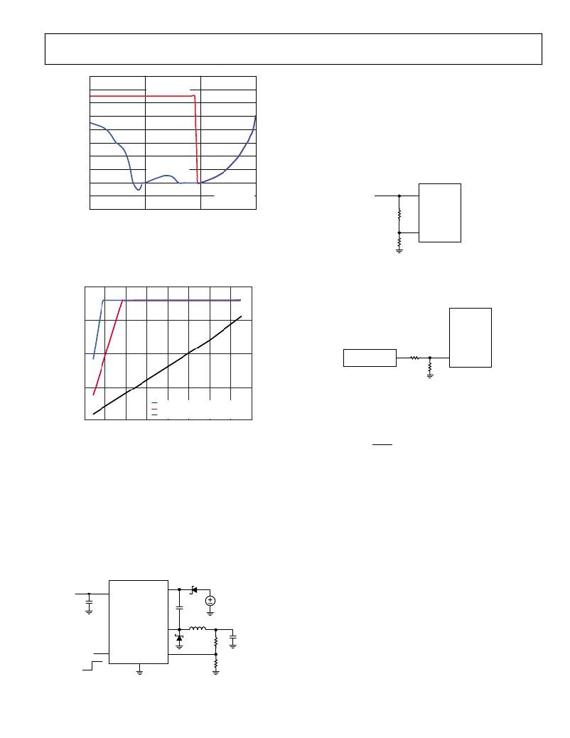
�Generally,� the� EN� pin� can� be� easily� tied� to� the� VIN� pin� so� that� the�
�device� automatically� starts� up� when� the� input� power� is� applied.�
�However,� the� precision� enable� feature� allows� the� ADP2300/�
�ADP2301� to� be� used� as� a� programmable� UVLO� by� connecting�
�a� resistive� voltage� divider� to� V� IN� ,� as� shown� in� Figure� 46.� This�
�configuration� prevents� the� start-up� problems� that� can� occur�
�when� V� IN� ramps� up� slowly� in� soft� start� with� a� relatively� high�
�load� current.�
�3.7�
�3.5�
�1�
�10�
�100�
�V� OUT� =� 3.3V�
�f� SW� =� 1.4MHz�
�1k�
�V� IN�
�R� EN1�
�VIN�
�ADP2300/�
�ADP2301�
�LOAD� CURRENT� (mA)�
�Figure� 43.� Minimum� Input� Voltage� vs.� Load� Current�
�R� EN2�
�EN�
�Based� on� three� conversion� limitations� (the� minimum� on� time,�
�the� minimum� off� time,� and� the� bootstrap� dropout� voltage),�
��22�
�Figure� 46.� Precision� Enable� Used� as� a� Programmable� UVLO�
�The� precision� enable� feature� also� allows� the� ADP2300/ADP2301� to�
�be� sequenced� precisely� by� using� a� resistive� voltage� divider� with�
��17�
�ADP2300/�
�ADP2301�
�12�
�OTHER� DC-TO-DC�
�OUTPUT�
�R� EN1�
�EN�
�R� EN2�
�7�
�Figure� 47.� Precision� Enable� Used� as� a� Sequencing� Control�
�from� Another� DC-to-DC� Output�
�2�
�0�
�2�
�4�
�6�
�MAXIMUM� INPUT� FOR� ADP2300�
�MAXIMUM� INPUT� FOR� ADP2301�
�MINIMUM� INPUT� FOR� ADP2300/ADP2301�
�8� 10� 12� 14�
�16�
�With� a� 1.2� μA� pull-down� current� on� the� EN� pin,� the� equation� for�
�the� start-up� voltage� in� Figure� 46� and� Figure� 47� is�
�V� STARTUP� =� ?� ?�
�+� 1� .� 2� μA� ?� ?� ×� R� EN� 1� +� 1� .� 2� V�
�V� OUT� (V)�
�Figure� 44.� Voltage� Conversion� Limitations�
�LOW� INPUT� VOLTAGE� CONSIDERATIONS�
�For� low� input� voltage� between� 3� V� and� 5� V,� the� internal� boot�
�regulator� cannot� provide� enough� 5.0� V� bootstrap� voltage� due� to�
�the� internal� dropout� voltage.� As� a� result,� the� increased� MOSFET�
�R� DS(ON)� reduces� the� available� load� current.� To� prevent� this,� add�
�an� external� small-signal� Schottky� diode� from� a� 5.0� V� external�
�bootstrap� bias� voltage.� Because� the� absolute� maximum� rating�
�between� the� BST� and� SW� pins� is� 6.0� V,� the� bias� voltage� should�
�be� less� than� 5.5� V.� Figure� 45� shows� the� application� diagram� for�
�the� external� bootstrap� circuit.�
�?� 1 . 2 V� ?�
�?� R� EN� 2� ?�
�where:�
�V� STARTUP� is� the� start-up� voltage� to� enable� the� chip.�
�R� EN1� is� the� resistor� from� the� dc� source� to� EN.�
�R� EN2� is� the� resistor� from� EN� to� GND.�
�3V� ~� 5V�
�VIN�
�BST�
�SCHOTTKY� DIODE�
�5V� BIAS�
�VOLTAGE�
�ADP2300/�
�ADP2301�
�SW�
�ON�
�EN�
�GND�
�FB�
�OFF�
�Figure� 45.� External� Bootstrap� Circuit� for� Low� Input� Voltage� Application�
�Rev.� C� |� Page� 17� of� 28�
�相关PDF资料 |
PDF描述 |
|---|---|
| IR2103STR | IC DRIVER HALF BRIDGE 600V 8SOIC |
| RCC18DCMI-S288 | CONN EDGECARD 36POS .100 EXTEND |
| EBM12DRYH-S13 | CONN EDGECARD 24POS .156 EXTEND |
| R1S-2405/EH | CONV DC/DC 1W 24VIN 05VOUT |
| VE-B6B-CW-F4 | CONVERTER MOD DC/DC 95V 100W |
相关代理商/技术参数 |
参数描述 |
|---|---|
| ADP2302 | 制造商:AD 制造商全称:Analog Devices 功能描述:Quad-Channel, 12-Bit, Serial Input, 4 mA to 20 mA |
| ADP2302_12 | 制造商:AD 制造商全称:Analog Devices 功能描述:2 A/3 A, 20 V, 700 kHz, Nonsynchronous Step-Down Regulators |
| ADP2302ARDZ | 功能描述:IC REG BUCK ADJ 2A 8SOIC RoHS:是 类别:集成电路 (IC) >> PMIC - 稳压器 - DC DC 开关稳压器 系列:- 标准包装:250 系列:- 类型:降压(降压) 输出类型:固定 输出数:1 输出电压:1.2V 输入电压:2.05 V ~ 6 V PWM 型:电压模式 频率 - 开关:2MHz 电流 - 输出:500mA 同步整流器:是 工作温度:-40°C ~ 85°C 安装类型:表面贴装 封装/外壳:6-UFDFN 包装:带卷 (TR) 供应商设备封装:6-SON(1.45x1) 产品目录页面:1032 (CN2011-ZH PDF) 其它名称:296-25628-2 |
| ADP2302ARDZ-2.5 | 制造商:Analog Devices 功能描述: |
| ADP2302ARDZ-2.5-R7 | 功能描述:IC REG BUCK 2.5V 2A 8SOIC RoHS:是 类别:集成电路 (IC) >> PMIC - 稳压器 - DC DC 开关稳压器 系列:- 标准包装:500 系列:- 类型:切换式电容器(充电泵),反相 输出类型:固定 输出数:1 输出电压:-3V 输入电压:2.3 V ~ 5.5 V PWM 型:Burst Mode? 频率 - 开关:900kHz 电流 - 输出:100mA 同步整流器:无 工作温度:-40°C ~ 85°C 安装类型:表面贴装 封装/外壳:SOT-23-6 细型,TSOT-23-6 包装:带卷 (TR) 供应商设备封装:TSOT-23-6 其它名称:LTC1983ES6-3#TRMTR |
发布紧急采购,3分钟左右您将得到回复。