- 您现在的位置:买卖IC网 > PDF目录16542 > ADP5585CP-EVALZ (Analog Devices Inc)BOARD EVAL FOR ADP5585CP PDF资料下载
参数资料
| 型号: | ADP5585CP-EVALZ |
| 厂商: | Analog Devices Inc |
| 文件页数: | 2/40页 |
| 文件大小: | 0K |
| 描述: | BOARD EVAL FOR ADP5585CP |
| 标准包装: | 1 |
| 主要目的: | 接口,GPIO 扩展器 |
| 已用 IC / 零件: | ADP5585 |
| 主要属性: | 10 个可配置的 I/O |
| 次要属性: | I²C 接口 |
| 已供物品: | 板 |
第1页当前第2页第3页第4页第5页第6页第7页第8页第9页第10页第11页第12页第13页第14页第15页第16页第17页第18页第19页第20页第21页第22页第23页第24页第25页第26页第27页第28页第29页第30页第31页第32页第33页第34页第35页第36页第37页第38页第39页第40页
ADP5585
Data Sheet
Rev. C | Page 10 of 40
1
23
4
56
7
89
VDD
R0
R1
R2
C2
C0
C1
3 × 3 KEYPAD MATRIX
09
84
1-
0
08
KEY
SCAN
CONTROL
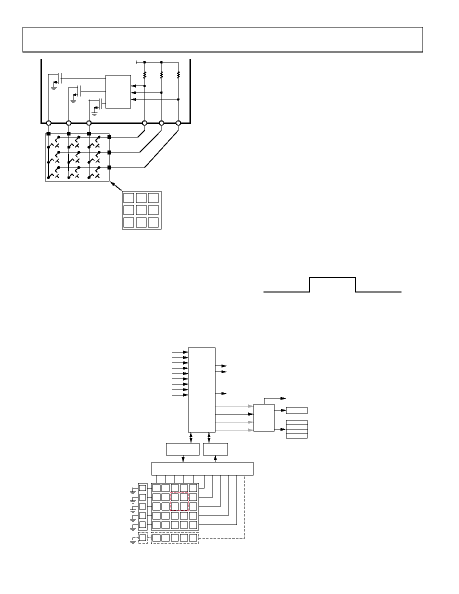
Figure 9. Simplified Key Scan Block
Figure 9 shows a simplified representation of the key scan block
using three row and three column pins connected to a small 3 × 3,
nine-switch keypad matrix. When the key scanner is idle, the
row pins are pulled high and the column pins are driven low.
The key scanner operates by checking the row pins to see if they
are low.
If Switch 6 in the matrix is pressed, R1 connects to C2. The key
scan circuit senses that one of the row pins has been pulled low,
and a key scan cycle begins. Key scanning involves driving all
column pins high, then driving each column pin, one at a time,
low and sensing whether a row pin is low or not. All row/column
pairs are scanned; therefore, if multiple keys are pressed, they
are detected.
To prevent glitches or narrow press times being registered as a
valid key press, the key scanner requires the key be pressed for
two scan cycles. The key scanner has a wait time between each
scan cycle; therefore, the key must be pressed and held for at
least this wait time to register as being pressed. If the key is
continuously pressed, the key scanner continues to scan, wait,
scan, wait, and so forth.
If Switch 6 is released, the connection between R1 and C2
breaks, and R1 is pulled up high. The key scanner requires that
the key be released for two scan cycles because the release of a
key is not necessarily in sync with the key scanner, it may take
up to two full wait/scan cycles for a key to register as released.
When the key is registered as released, and no other keys are
pressed, the key scanner returns to idle mode.
For the remainder of this document, the press/release status of a
key is represented as simply a logic signal in the figures. A logic
high level represents the key status as pressed, and a logic low
represents released. This eliminates the need to draw individual
row/column signals when describing key events.
KEY x
KEY RELEASED
KEY PRESSED
0
9841-
009
Figure 10. Logic Low: Released, Logic High: Pressed
Figure 11 shows a detailed representation of the key scan block
and its associated control and status signals. When all row and
column pins are used, a matrix of 25 unique keys can be
scanned.
LOGIC EVENT
5
4
3
2
1
10
9
8
7
6
15
14
13
12
11
20
19
18
17
16
25
24
23
22
21
30
29
28
27
26
I/O CONFIGURATION
KEY EVENT
GPI EVENT
I2C BUSY?
R0
R3
R1 R2
R4 R5
C0 C1 C2 C3 C4
PIN_CONFIG_A[7:0]
PIN_CONFIG_B[7:0]
FIFO
PIN_CONFIG_C[7:0]
EVENT_INT
OVRFLOW_INT
EC[4:0]
RESET_TRIG_TIME[2:0]
RESET1_EVENT_A[7:0]
RESET1_EVENT_B[7:0]
RESET1_EVENT_C[7:0]
31
33
36
32
35
34
RESET2_EVENT_A[7:0]
RESET2_EVENT_B[7:0]
RESET 1_INITIATE
RESET 2_INITIATE
09
84
1-
01
0
FIFO
UPDATE
KEY SCAN
CONTROL
COLUMN
SINK ON/OFF
ROW
SENSE
Figure 11. Detailed Key Scan Block
相关PDF资料 |
PDF描述 |
|---|---|
| EBM25DSEF-S13 | CONN EDGECARD 50POS .156 EXTEND |
| GSC06DRTH-S734 | CONN EDGECARD 12POS DIP .100 SLD |
| 5503995-4 | CABLE ASSEM FIBER ST-ST 5 METER |
| ADA4853-3YRU-EBZ | BOARD EVAL FOR ADA4853-3YRU |
| A3CCB-2636G | IDC CABLE- AKC26B/AE26G/AKC26B |
相关代理商/技术参数 |
参数描述 |
|---|---|
| ADP5586 | 制造商:AD 制造商全称:Analog Devices 功能描述:Keypad Decoder and I/O Port Expander |
| ADP5586ACBZ-00-R7 | 功能描述:接口-I/O扩展器 RoHS:否 制造商:NXP Semiconductors 逻辑系列: 输入/输出端数量: 最大工作频率:100 kHz 工作电源电压:1.65 V to 5.5 V 工作温度范围:- 40 C to + 85 C 安装风格:SMD/SMT 封装 / 箱体:HVQFN-16 封装:Reel |
| ADP5586ACBZ-01-R7 | 功能描述:接口-I/O扩展器 RoHS:否 制造商:NXP Semiconductors 逻辑系列: 输入/输出端数量: 最大工作频率:100 kHz 工作电源电压:1.65 V to 5.5 V 工作温度范围:- 40 C to + 85 C 安装风格:SMD/SMT 封装 / 箱体:HVQFN-16 封装:Reel |
| ADP5586ACBZ-03-R7 | 功能描述:接口-I/O扩展器 RoHS:否 制造商:NXP Semiconductors 逻辑系列: 输入/输出端数量: 最大工作频率:100 kHz 工作电源电压:1.65 V to 5.5 V 工作温度范围:- 40 C to + 85 C 安装风格:SMD/SMT 封装 / 箱体:HVQFN-16 封装:Reel |
| ADP5586CB-EVALZ | 功能描述:界面开发工具 RoHS:否 制造商:Bourns 产品:Evaluation Boards 类型:RS-485 工具用于评估:ADM3485E 接口类型:RS-485 工作电源电压:3.3 V |
发布紧急采购,3分钟左右您将得到回复。