- 您现在的位置:买卖IC网 > PDF目录16542 > ADP5585CP-EVALZ (Analog Devices Inc)BOARD EVAL FOR ADP5585CP PDF资料下载
参数资料
| 型号: | ADP5585CP-EVALZ |
| 厂商: | Analog Devices Inc |
| 文件页数: | 6/40页 |
| 文件大小: | 0K |
| 描述: | BOARD EVAL FOR ADP5585CP |
| 标准包装: | 1 |
| 主要目的: | 接口,GPIO 扩展器 |
| 已用 IC / 零件: | ADP5585 |
| 主要属性: | 10 个可配置的 I/O |
| 次要属性: | I²C 接口 |
| 已供物品: | 板 |
第1页第2页第3页第4页第5页当前第6页第7页第8页第9页第10页第11页第12页第13页第14页第15页第16页第17页第18页第19页第20页第21页第22页第23页第24页第25页第26页第27页第28页第29页第30页第31页第32页第33页第34页第35页第36页第37页第38页第39页第40页
ADP5585
Data Sheet
Rev. C | Page 14 of 40
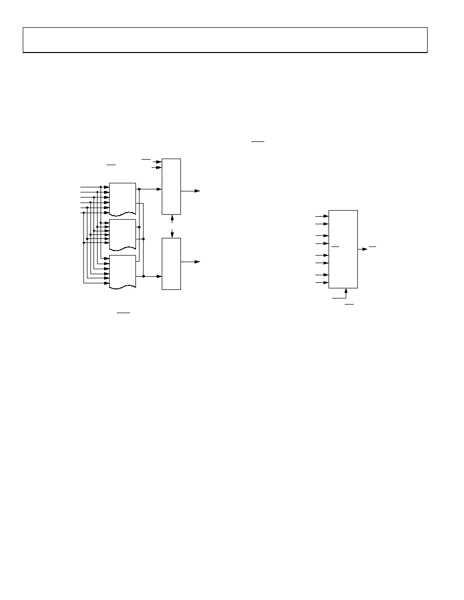
RESET BLOCKS
ADP5585 features two reset blocks that can generate reset con-
ditions if certain events are detected simultaneously. Up to three
reset trigger events can be programmed for RESET1. Up to two
reset trigger events can be programmed for RESET2. The event
scan control blocks monitor whether these events are present for
the duration of RESET_TRIG_TIME[2:0] (Register 0x2E,
Bits[4:2]). If they are, reset-initiate signals are sent to the reset
generator blocks. The generated reset signal pulse width is
programmable.
RESET_PULSE_WIDTH[1:0]
RESET_TRIG_TIME[2:0]
RESET1_EVENT_A[7:0]
RESET1_EVENT_B[7:0]
RESET1_EVENT_C[7:0]
KEY
SCAN
CONTROL
RST_PASSTHRU_EN
RST
(R4)
RESET1
GPI
SCAN
CONTROL
LOGIC
BLOCK
CONTROL
RESET2_EVENT_A[7:0]
RESET2_EVENT_B[7:0]
(C4)
RESET2
RESET1_
INITIATE
RESET2_
INITIATE
RESET
GEN 2
RESET
GEN 1
09841-
020
Figure 21. Reset Blocks
The Reset 1 signal uses the R4 I/O pin as its output. A pass
through mode allows the main RST pin to be output on the R4
pin also. The Reset 2 signal uses the C4 I/O pin as its output.
The reset generation signals are useful in situations where the
system processor has locked up and the system is unresponsive
to input events. The user can press one of the reset event combi-
nations and initiate a system wide reset. This alleviates the need
for removing the battery from the system and doing a hard reset.
It is not recommended to use the immediate trigger time (see
Table 54) because this setting may cause false triggering.
Interrupts
The INT pin can be asserted low if any of the internal interrupt
sources is active. The user can select which internal interrupts
interact with the external interrupt pin in Register 0x3C (refer
to Table 68). Register 0x3B allows the user to choose whether
the external interrupt pin remains asserted, or deasserts for
50 s, then reasserts, in the case that there are multiple internal
interrupts asserted and one is cleared (refer to Table 67).
EVENT_INT
EVENT_IEN
INT DRIVE
INT
INT_CFG
GPI_INT
GPI_IEN
LOGIC_INT
LOGIC_IEN
OVRFLOW_INT
OVRFLOW_IEN
09841-
021
Figure 22. Asserting INT Low
相关PDF资料 |
PDF描述 |
|---|---|
| EBM25DSEF-S13 | CONN EDGECARD 50POS .156 EXTEND |
| GSC06DRTH-S734 | CONN EDGECARD 12POS DIP .100 SLD |
| 5503995-4 | CABLE ASSEM FIBER ST-ST 5 METER |
| ADA4853-3YRU-EBZ | BOARD EVAL FOR ADA4853-3YRU |
| A3CCB-2636G | IDC CABLE- AKC26B/AE26G/AKC26B |
相关代理商/技术参数 |
参数描述 |
|---|---|
| ADP5586 | 制造商:AD 制造商全称:Analog Devices 功能描述:Keypad Decoder and I/O Port Expander |
| ADP5586ACBZ-00-R7 | 功能描述:接口-I/O扩展器 RoHS:否 制造商:NXP Semiconductors 逻辑系列: 输入/输出端数量: 最大工作频率:100 kHz 工作电源电压:1.65 V to 5.5 V 工作温度范围:- 40 C to + 85 C 安装风格:SMD/SMT 封装 / 箱体:HVQFN-16 封装:Reel |
| ADP5586ACBZ-01-R7 | 功能描述:接口-I/O扩展器 RoHS:否 制造商:NXP Semiconductors 逻辑系列: 输入/输出端数量: 最大工作频率:100 kHz 工作电源电压:1.65 V to 5.5 V 工作温度范围:- 40 C to + 85 C 安装风格:SMD/SMT 封装 / 箱体:HVQFN-16 封装:Reel |
| ADP5586ACBZ-03-R7 | 功能描述:接口-I/O扩展器 RoHS:否 制造商:NXP Semiconductors 逻辑系列: 输入/输出端数量: 最大工作频率:100 kHz 工作电源电压:1.65 V to 5.5 V 工作温度范围:- 40 C to + 85 C 安装风格:SMD/SMT 封装 / 箱体:HVQFN-16 封装:Reel |
| ADP5586CB-EVALZ | 功能描述:界面开发工具 RoHS:否 制造商:Bourns 产品:Evaluation Boards 类型:RS-485 工具用于评估:ADM3485E 接口类型:RS-485 工作电源电压:3.3 V |
发布紧急采购,3分钟左右您将得到回复。