- 您现在的位置:买卖IC网 > PDF目录16542 > ADP5585CP-EVALZ (Analog Devices Inc)BOARD EVAL FOR ADP5585CP PDF资料下载
参数资料
| 型号: | ADP5585CP-EVALZ |
| 厂商: | Analog Devices Inc |
| 文件页数: | 39/40页 |
| 文件大小: | 0K |
| 描述: | BOARD EVAL FOR ADP5585CP |
| 标准包装: | 1 |
| 主要目的: | 接口,GPIO 扩展器 |
| 已用 IC / 零件: | ADP5585 |
| 主要属性: | 10 个可配置的 I/O |
| 次要属性: | I²C 接口 |
| 已供物品: | 板 |
第1页第2页第3页第4页第5页第6页第7页第8页第9页第10页第11页第12页第13页第14页第15页第16页第17页第18页第19页第20页第21页第22页第23页第24页第25页第26页第27页第28页第29页第30页第31页第32页第33页第34页第35页第36页第37页第38页当前第39页第40页
ADP5585
Data Sheet
Rev. C | Page 8 of 40
DEVICE ENABLE
When sufficient voltage is applied to VDD and the RST pin is
driven with a logic high level, the ADP5585 starts up in standby
mode with all settings at default. The user can configure the
device via the I2C interface. When the RST pin is low, the
ADP5585 enters a reset state and all settings return to default.
The RST pin features a debounce filter.
If using the ADP5585ACBZ-01-R7 or ADP5585ACPZ-01-R7
device model, the RST pin acts as an extra row pin. Without a
reset pin, the only method to reset the device is by bringing
VDD below the UVLO threshold.
DEVICE OVERVIEW
The ADP5585 contains 10 multiconfigurable input/output pins.
Each pin can be programmed to enable the device to carry out
its various functions, as follows:
Keypad matrix decoding (five-column by five-row matrix
maximum).
General-purpose I/O expansion (up to 10 inputs/outputs).
PWM generation.
Logic function building blocks (up to three inputs and one
output).
Two reset generators.
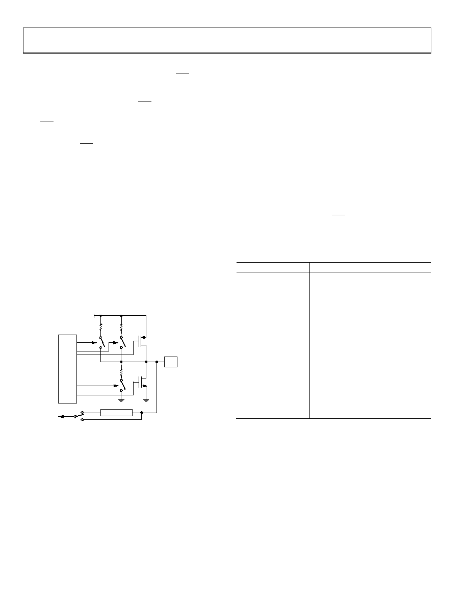
All 10 input/output pins have an I/O structure as shown in
I/O
VDD
100k
DEBOUNCE
300k
09841-
005
I/O
DRIVE
Figure 6. I/O Structure
Each I/O can be pulled up with a 100 kΩ or 300 kΩ resistor or
pulled down with a 300 kΩ resistor. For logic output drive, each
I/O has a 5 mA PMOS source and a 10 mA NMOS sink for a push-
pull type output. For open-drain output situations, the 5 mA
PMOS source is not enabled. For logic input applications, each
I/O can be sampled directly or, alternatively, sampled through a
debounce filter.
The I/O structure shown in Figure 6 allows for all GPI and GPO
functions, as well as PWM and clock divide functions. For key
matrix scan and decode, the scanning circuit uses the 100 kΩ or
300 kΩ resistor for pulling up keypad row pins and the 10 mA
NMOS sinks for grounding keypad column pins (see the Key
Scan Control section for details about key decoding).
Configuration of the device is carried out by programming an
array of internal registers via the I2C interface. Feedback of
device status and pending interrupts can be flagged to an
external processor by using the INT pin.
The ADP5585 is offered with three feature sets. Table 5 lists the
options that are available for each model of the ADP5585.
Table 5. Matrix Options by Device Model
Model
Description
ADP5585ACBZ-00-R7
GPIO pull up (default option)
5-row × 5-column matrix
ADP5585ACBZ-01-R7
Row 5 added to GPIOs
6-row × 5-column matrix
ADP5585ACBZ-02-R7
No pull-up resistors to special function
pins1
5-row × 5-column matrix
ADP5585ACBZ-04-R7
Pull-down resistors to all GPIO pins on
start-up
5-row × 5-column matrix
ADP5585ACPZ-00-R7
GPIO pull up (default option)
5-row × 5-column matrix
ADP5585ACPZ-01-R7
Row 5 added to GPIOs
6-row × 5-column matrix
ADP5585ACPZ-03-R7
Alternate I2C address (0x30)
5-row × 5-column matrix
1
Special function pins are defined as R0, R3, R4, and C4. See Table 4 for
details.
相关PDF资料 |
PDF描述 |
|---|---|
| EBM25DSEF-S13 | CONN EDGECARD 50POS .156 EXTEND |
| GSC06DRTH-S734 | CONN EDGECARD 12POS DIP .100 SLD |
| 5503995-4 | CABLE ASSEM FIBER ST-ST 5 METER |
| ADA4853-3YRU-EBZ | BOARD EVAL FOR ADA4853-3YRU |
| A3CCB-2636G | IDC CABLE- AKC26B/AE26G/AKC26B |
相关代理商/技术参数 |
参数描述 |
|---|---|
| ADP5586 | 制造商:AD 制造商全称:Analog Devices 功能描述:Keypad Decoder and I/O Port Expander |
| ADP5586ACBZ-00-R7 | 功能描述:接口-I/O扩展器 RoHS:否 制造商:NXP Semiconductors 逻辑系列: 输入/输出端数量: 最大工作频率:100 kHz 工作电源电压:1.65 V to 5.5 V 工作温度范围:- 40 C to + 85 C 安装风格:SMD/SMT 封装 / 箱体:HVQFN-16 封装:Reel |
| ADP5586ACBZ-01-R7 | 功能描述:接口-I/O扩展器 RoHS:否 制造商:NXP Semiconductors 逻辑系列: 输入/输出端数量: 最大工作频率:100 kHz 工作电源电压:1.65 V to 5.5 V 工作温度范围:- 40 C to + 85 C 安装风格:SMD/SMT 封装 / 箱体:HVQFN-16 封装:Reel |
| ADP5586ACBZ-03-R7 | 功能描述:接口-I/O扩展器 RoHS:否 制造商:NXP Semiconductors 逻辑系列: 输入/输出端数量: 最大工作频率:100 kHz 工作电源电压:1.65 V to 5.5 V 工作温度范围:- 40 C to + 85 C 安装风格:SMD/SMT 封装 / 箱体:HVQFN-16 封装:Reel |
| ADP5586CB-EVALZ | 功能描述:界面开发工具 RoHS:否 制造商:Bourns 产品:Evaluation Boards 类型:RS-485 工具用于评估:ADM3485E 接口类型:RS-485 工作电源电压:3.3 V |
发布紧急采购,3分钟左右您将得到回复。