参数资料
| 型号: | ADS1259BIPWR |
| 厂商: | Texas Instruments |
| 文件页数: | 17/48页 |
| 文件大小: | 0K |
| 描述: | IC ADC 24BIT SPI 14KSPS 20TSSOP |
| 标准包装: | 2,000 |
| 位数: | 24 |
| 采样率(每秒): | 14k |
| 数据接口: | 串行,SPI? |
| 转换器数目: | 1 |
| 电压电源: | 模拟和数字,双 ± |
| 工作温度: | -40°C ~ 125°C |
| 安装类型: | 表面贴装 |
| 封装/外壳: | 20-TSSOP(0.173",4.40mm 宽) |
| 供应商设备封装: | 20-TSSOP |
| 包装: | 带卷 (TR) |
| 输入数目和类型: | 2 个单端,单极;2 个单端,双极;1 个差分,单极;1 个差分,双极 |
第1页第2页第3页第4页第5页第6页第7页第8页第9页第10页第11页第12页第13页第14页第15页第16页当前第17页第18页第19页第20页第21页第22页第23页第24页第25页第26页第27页第28页第29页第30页第31页第32页第33页第34页第35页第36页第37页第38页第39页第40页第41页第42页第43页第44页第45页第46页第47页第48页
STARTPin
DRDY
Halted
Single
Conversion
Halted
Single
Conversion
OR
START
DRDY
DOUT
Settled
Data
START
Pin
START
Command
or
t
SET
(1)
7thFallingSCLKEdgeofOpcode
V
=AINP
AINN
-
IN
SettledV
IN
SBAS424D
– JUNE 2009 – REVISED AUGUST 2011
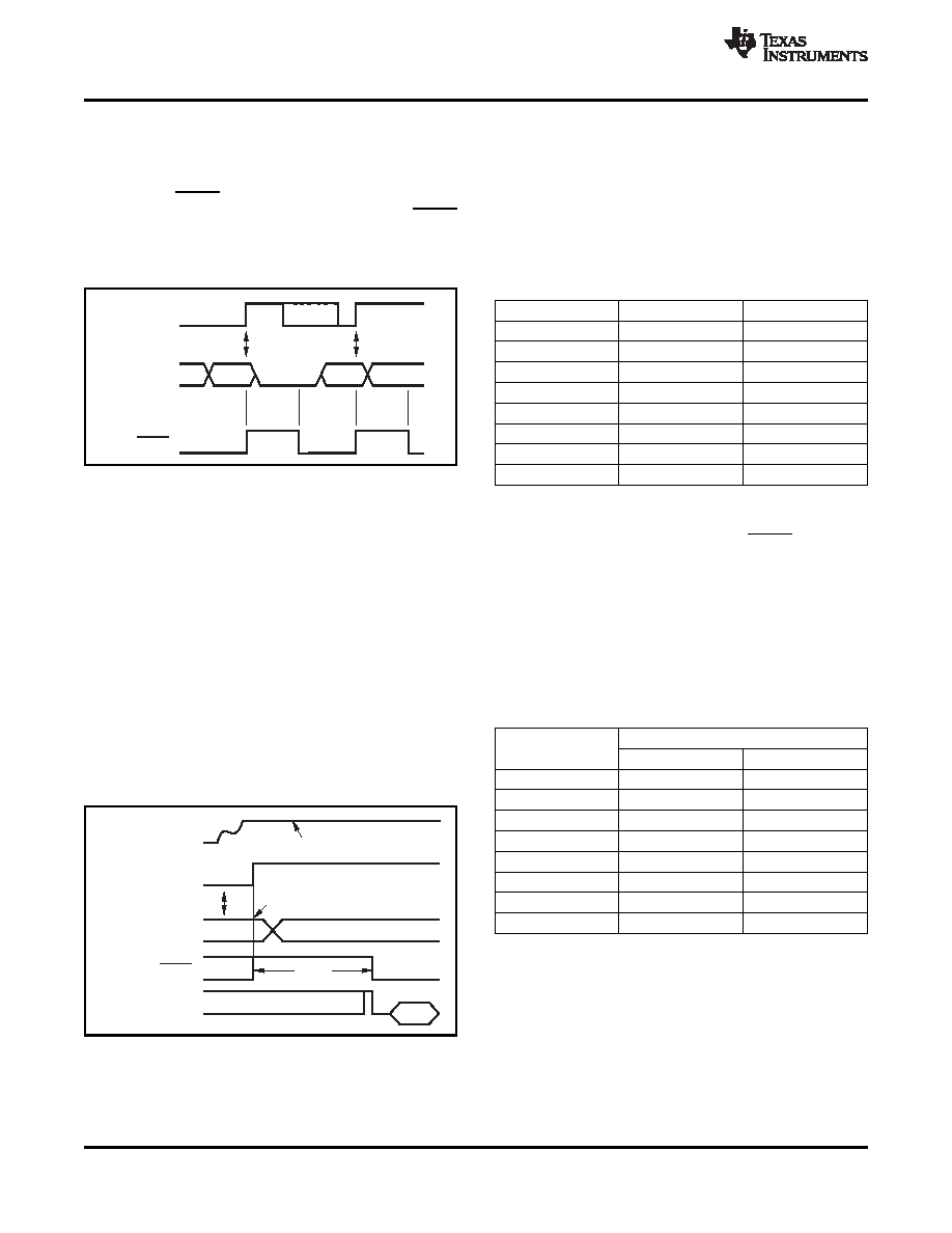
Pulse Control Mode (PULSE Bit = 1)
Settling Time Using START
In the Pulse Control mode, the ADS1259 performs a
When START goes high (via pin or command) a
single conversion when either the START pin is taken
delay may be programmed before the conversion
high or when the START command is sent. As seen
filter cycle begins. The programmable delay may be
in Figure 52, DRDY goes high when the conversion is
useful to provide time for external circuits (such as
started. When the conversion is complete, DRDY
after an external signal mux change), before the
goes low and further conversions are halted. To start
reading is started. Register bits DELAY[2:0] set the
a new conversion, transition the START pin back to
initial delay time as shown in Table 8.
high, or transmit the START opcode again.
Table 8. Initial START Delay
DELAY[2:0]
tDELAY (tCLK)
000
0
001
64
8.68
010
128
17.4
011
256
34.7
100
512
69.4
101
1024
139
110
2048
278
111
4096
556
(1) START opcode command takes effect on the seventh SCLK
falling edge.
(1) fCLK = 7.3728MHz.
Figure 52. Pulse Control Mode
After the programmable delay, the digital filter is reset
and a new conversion is started. DRDY goes low
when data are ready. There is no need to ignore or
CONVERSION SETTLING TIME
discard data; the data are completely settled. The
total time to perform the first conversion is the sum of
The ADS1259 features a digital filter architecture in
the programmable delay time and the settling of the
which settling time can be traded for wide filter
notches, resulting in improved line-cycle rejection.
This trade-off is determined by the selection of the
shows the settling time with programmable delay
sinc1 or sinc2 filter. The sinc1 filter settles in a single
equal to '0'.
cycle while the sinc2 filter provides wide-width filter
notches. The settling time of the ADS1259 is different
Table 9. Settling Time Using START
if START is used to begin conversions or if the
ADS1259 is free-running the conversions. These
DATA RATE
modes are explained in the Settling Time Using
(SPS)
sinc1
sinc2
and
10
100
200
Converting sections.
16.6
60.3
120
50
20.3
40.4
60
17.0
33.7
400
2.85
5.42
1200
1.18
2.10
3600
0.632
0.980
14,400
0.424
0.563
(1) fCLK = 7.3728MHz, DELAY[2:0] = 000.
(1) tSET = initial start delay plus the new conversion cycle time.
Figure 53. Data Retrieval Time After START
24
Copyright
2009–2011, Texas Instruments Incorporated
相关PDF资料 |
PDF描述 |
|---|---|
| ADS1286UB/2K5G4 | IC ADC 12BIT SPI 37KSPS 8SOIC |
| ADS1601IPFBTG4 | IC ADC 16BIT 1.25MSPS 48-TQFP |
| ADS62C17IRGC25 | IC ADC 11BIT 200MSPS DUAL 64VQFN |
| ADS62P45IRGC25 | IC ADC 14B SER/PAR 125M 64VQFN |
| ADS7812U/1KE4 | IC 12BIT 35MW SER OUT ADC 16SOIC |
相关代理商/技术参数 |
参数描述 |
|---|---|
| ADS1259EVM | 功能描述:数据转换 IC 开发工具 ADS1259 Eval Mod RoHS:否 制造商:Texas Instruments 产品:Demonstration Kits 类型:ADC 工具用于评估:ADS130E08 接口类型:SPI 工作电源电压:- 6 V to + 6 V |
| ADS1259EVM | 制造商:Texas Instruments 功能描述:DEVELOPMENT TOOL |
| ADS1259EVM-PDK | 功能描述:数据转换 IC 开发工具 ADS1259 Perf Demo Kit RoHS:否 制造商:Texas Instruments 产品:Demonstration Kits 类型:ADC 工具用于评估:ADS130E08 接口类型:SPI 工作电源电压:- 6 V to + 6 V |
| ADS1259EVM-PDK | 制造商:Texas Instruments 功能描述:DEVELOPMENT TOOL |
| ADS1259IPW | 功能描述:模数转换器 - ADC Low-Noise 14kSPS 24B ADC RoHS:否 制造商:Texas Instruments 通道数量:2 结构:Sigma-Delta 转换速率:125 SPs to 8 KSPs 分辨率:24 bit 输入类型:Differential 信噪比:107 dB 接口类型:SPI 工作电源电压:1.7 V to 3.6 V, 2.7 V to 5.25 V 最大工作温度:+ 85 C 安装风格:SMD/SMT 封装 / 箱体:VQFN-32 |
发布紧急采购,3分钟左右您将得到回复。