参数资料
| 型号: | ADS1259BIPWR |
| 厂商: | Texas Instruments |
| 文件页数: | 36/48页 |
| 文件大小: | 0K |
| 描述: | IC ADC 24BIT SPI 14KSPS 20TSSOP |
| 标准包装: | 2,000 |
| 位数: | 24 |
| 采样率(每秒): | 14k |
| 数据接口: | 串行,SPI? |
| 转换器数目: | 1 |
| 电压电源: | 模拟和数字,双 ± |
| 工作温度: | -40°C ~ 125°C |
| 安装类型: | 表面贴装 |
| 封装/外壳: | 20-TSSOP(0.173",4.40mm 宽) |
| 供应商设备封装: | 20-TSSOP |
| 包装: | 带卷 (TR) |
| 输入数目和类型: | 2 个单端,单极;2 个单端,双极;1 个差分,单极;1 个差分,双极 |
第1页第2页第3页第4页第5页第6页第7页第8页第9页第10页第11页第12页第13页第14页第15页第16页第17页第18页第19页第20页第21页第22页第23页第24页第25页第26页第27页第28页第29页第30页第31页第32页第33页第34页第35页当前第36页第37页第38页第39页第40页第41页第42页第43页第44页第45页第46页第47页第48页
50W
PGA
MUX
2
3
1
4.7kW
(2)
18
19
24
1 F
m
10nF
(3)
1MW
100kW
VOP
VOCM
VON
GPIO6
GPIO5
GPIO0
12
8
DGND
VSON
DVDD
SCLK
SDO
SDI
C
S
INN2
7
INP2
10
INN1
9
INP1
VSP
+15V
(1)
+5V
+3.3V
6
17
19
15
14
11
12
13
15
14
16
13
5
(1)
VSN
-15V
(1)
11
VSOP
4
(1)
3
10
8
9
7
6
1 F
m
1 F
m
1 F
m
RESETPWDN
/
DRDY
AINP
REFOUT
AINN
SYNCOUT
START
DIN
DOUT
SCLK
CS
4
5
B
YP
AS
S
XT
AL2
XT
AL1
DGND
DVDD
A
VS
S
2
16
1
AVDD
20
VREFP
17
VREFN
18
PGA280
ADS1259
Controller
SPI
1 F
m
+
SBAS424D
– JUNE 2009 – REVISED AUGUST 2011
3. Optional readback verification of the register data
READ register command:
<20h>, <08>
The nine bytes of readback data that follow represent the nine register bytes.
4. Take the START pin high or send the START command to start conversions.
5. Optionally, send the RDATAC command
<10h>. This permits reading of conversion data without the need of
the read data command. Otherwise, the read data opcode must be sent to read each conversion result.
6. When the DRDY pin or the DRDY bit goes low, or when DOUT transitions low, read the data.
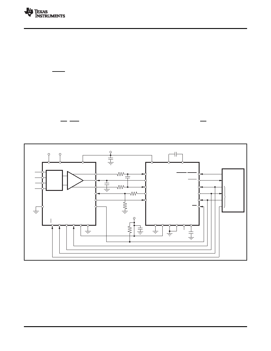
PGA280 APPLICATION
Figure 65 shows the ADS1259 connected to the PGA280. The PGA280 is a programmable gain, fully-differential
instrumentation amplifier that is ideally suited to drive the ADS1259. The amplifier features
±5V to ±18V supply
input section that accepts wide ranging signal levels and features a +5V output section that matches the
ADS1259 low-voltage inputs. The ADS1259 +2.5V REFOUT drives the PGA280 VOCM pin to level shift the
signal.
The ADS1259 provides a clock output (SYNCOUT) that drives the PGA280 (GPIO6) chopping clock input. An
optional extended CS (ECS) function feature of the PGA280 (GPIO0) allows use of one CS to alternately select
each device for SPI communication. Additionally, the optional BUFA trigger output of the PGA280 (GPIO5) starts
the ADS1259 conversions. The trigger can be delayed to occur after an input multiplexer change. The delay
allows settling of the PGA280 before the ADC conversion begins.
(1) Refer to the PGA280 product data sheet for power-supply bypassing recommendations.
(2) Locate this resistor as close as possible to pin 5 of the ADS1259.
(3) C0G or film capacitor.
Figure 65. PGA280 Driving the ADS1259
Copyright
2009–2011, Texas Instruments Incorporated
41
相关PDF资料 |
PDF描述 |
|---|---|
| ADS1286UB/2K5G4 | IC ADC 12BIT SPI 37KSPS 8SOIC |
| ADS1601IPFBTG4 | IC ADC 16BIT 1.25MSPS 48-TQFP |
| ADS62C17IRGC25 | IC ADC 11BIT 200MSPS DUAL 64VQFN |
| ADS62P45IRGC25 | IC ADC 14B SER/PAR 125M 64VQFN |
| ADS7812U/1KE4 | IC 12BIT 35MW SER OUT ADC 16SOIC |
相关代理商/技术参数 |
参数描述 |
|---|---|
| ADS1259EVM | 功能描述:数据转换 IC 开发工具 ADS1259 Eval Mod RoHS:否 制造商:Texas Instruments 产品:Demonstration Kits 类型:ADC 工具用于评估:ADS130E08 接口类型:SPI 工作电源电压:- 6 V to + 6 V |
| ADS1259EVM | 制造商:Texas Instruments 功能描述:DEVELOPMENT TOOL |
| ADS1259EVM-PDK | 功能描述:数据转换 IC 开发工具 ADS1259 Perf Demo Kit RoHS:否 制造商:Texas Instruments 产品:Demonstration Kits 类型:ADC 工具用于评估:ADS130E08 接口类型:SPI 工作电源电压:- 6 V to + 6 V |
| ADS1259EVM-PDK | 制造商:Texas Instruments 功能描述:DEVELOPMENT TOOL |
| ADS1259IPW | 功能描述:模数转换器 - ADC Low-Noise 14kSPS 24B ADC RoHS:否 制造商:Texas Instruments 通道数量:2 结构:Sigma-Delta 转换速率:125 SPs to 8 KSPs 分辨率:24 bit 输入类型:Differential 信噪比:107 dB 接口类型:SPI 工作电源电压:1.7 V to 3.6 V, 2.7 V to 5.25 V 最大工作温度:+ 85 C 安装风格:SMD/SMT 封装 / 箱体:VQFN-32 |
发布紧急采购,3分钟左右您将得到回复。