- 您现在的位置:买卖IC网 > PDF目录19376 > ADSP-2101BG-100 (Analog Devices Inc)IC DSP CONTROLLER 16BIT 68PGA PDF资料下载
参数资料
| 型号: | ADSP-2101BG-100 |
| 厂商: | Analog Devices Inc |
| 文件页数: | 13/64页 |
| 文件大小: | 0K |
| 描述: | IC DSP CONTROLLER 16BIT 68PGA |
| 标准包装: | 1 |
| 系列: | ADSP-21xx |
| 类型: | 定点 |
| 接口: | 同步串行端口(SSP) |
| 时钟速率: | 25MHz |
| 非易失内存: | 外部 |
| 芯片上RAM: | 6kB |
| 电压 - 输入/输出: | 5.00V |
| 电压 - 核心: | 5.00V |
| 工作温度: | -40°C ~ 85°C |
| 安装类型: | 通孔 |
| 封装/外壳: | 68-BEPGA |
| 供应商设备封装: | 68-PGA(27.89x27.89) |
| 包装: | 托盘 |
第1页第2页第3页第4页第5页第6页第7页第8页第9页第10页第11页第12页当前第13页第14页第15页第16页第17页第18页第19页第20页第21页第22页第23页第24页第25页第26页第27页第28页第29页第30页第31页第32页第33页第34页第35页第36页第37页第38页第39页第40页第41页第42页第43页第44页第45页第46页第47页第48页第49页第50页第51页第52页第53页第54页第55页第56页第57页第58页第59页第60页第61页第62页第63页第64页
ADSP-21xx
–20–
REV. B
TEST CONDITIONS
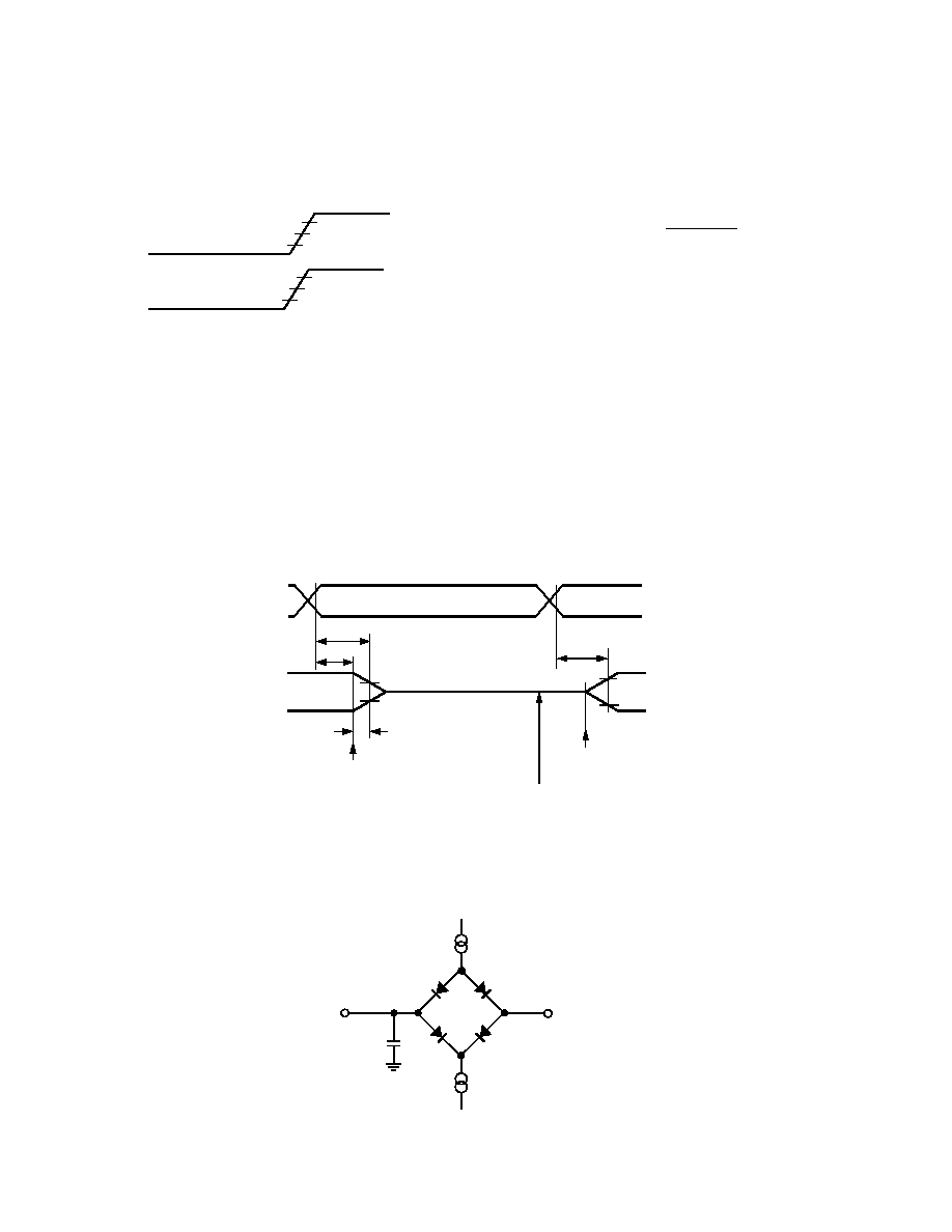
Figure 14 shows voltage reference levels for ac measurements.
Figure 14. Voltage Reference Levels for AC Measurements
(Except Output Enable/Disable)
Output Disable Time
Output pins are considered to be disabled when they have
stopped driving and started a transition from the measured
output high or low voltage to a high impedance state. The
output disable time (tDIS) is the difference of tMEASURED and
tDECAY, as shown in Figure 15. The time tMEASURED is the
interval from when a reference signal reaches a high or low
voltage level to when the output voltages have changed by 0.5 V
from the measured output high or low voltage.
The decay time, tDECAY, is dependent on the capacitative load,
CL, and the current load, iL, on the output pin. It can be
approximated by the following equation:
t
DECAY =
C
L × 0.5 V
i
L
from which
tDIS = tMEASURED – tDECAY
is calculated. If multiple pins (such as the data bus) are dis-
abled, the measurement value is that of the last pin to stop
driving.
Output Enable Time
Output pins are considered to be enabled when they have made
a transition from a high-impedance state to when they start
driving. The output enable time (t ENA) is the interval from
when a reference signal reaches a high or low voltage level to
when the output has reached a specified high or low trip point,
as shown in Figure 15. If multiple pins (such as the data bus)
are enabled, the measurement value is that of the first pin to
start driving.
SPECIFICATIONS (ADSP-2101/2105/2115/2161/2163)
3.0V
1.5V
0.0V
2.0V
1.5V
0.8V
INPUT
OUTPUT
Figure 15. Output Enable/Disable
TO
OUTPUT
PIN
50pF
+1.5V
IOH
IOL
Figure 16. Equivalent Device Loading for AC Measurements
(Except Output Enable/Disable)
2.0V
1.0V
t
ENA
REFERENCE
SIGNAL
OUTPUT
t
DECAY
VOH (MEASURED)
OUTPUT STOPS
DRIVING
OUTPUT STARTS
DRIVING
t
DIS
t
MEASURED
VOL (MEASURED)
VOH (MEASURED) – 0.5V
VOL (MEASURED) +0.5V
HIGH-IMPEDANCE STATE.
TEST CONDITIONS CAUSE
THIS VOLTAGE LEVEL TO BE
APPROXIMATELY 1.5V.
VOH (MEASURED)
VOL (MEASURED)
相关PDF资料 |
PDF描述 |
|---|---|
| VI-B2Z-CX-F4 | CONVERTER MOD DC/DC 2V 30W |
| DSEP30-06BR | DIODE 600V 30A ISOPLUS247 |
| TAJY107M016Y | CAP TANT 100UF 16V 20% 2917 |
| VI-B2Z-CW-F3 | CONVERTER MOD DC/DC 2V 40W |
| ADSP-21061LKB-160 | IC DSP CONTROLLER 32BIT 225BGA |
相关代理商/技术参数 |
参数描述 |
|---|---|
| ADSP-2101BG-40 | 制造商:Rochester Electronics LLC 功能描述:- Bulk |
| ADSP-2101BG-50 | 制造商:Analog Devices 功能描述: |
| ADSP-2101BG-66 | 制造商:AD 制造商全称:Analog Devices 功能描述:ADSP-2100 Family DSP Microcomputers |
| ADSP-2101BG-80 | 制造商:AD 制造商全称:Analog Devices 功能描述:ADSP-2100 Family DSP Microcomputers |
| ADSP-2101BGZ-100 | 制造商:Analog Devices 功能描述:DSP FIX PT 16BIT 25MHZ 25MIPS 68CPGA - Trays |
发布紧急采购,3分钟左右您将得到回复。