- 您现在的位置:买卖IC网 > PDF目录19376 > ADSP-2101BG-100 (Analog Devices Inc)IC DSP CONTROLLER 16BIT 68PGA PDF资料下载
参数资料
| 型号: | ADSP-2101BG-100 |
| 厂商: | Analog Devices Inc |
| 文件页数: | 2/64页 |
| 文件大小: | 0K |
| 描述: | IC DSP CONTROLLER 16BIT 68PGA |
| 标准包装: | 1 |
| 系列: | ADSP-21xx |
| 类型: | 定点 |
| 接口: | 同步串行端口(SSP) |
| 时钟速率: | 25MHz |
| 非易失内存: | 外部 |
| 芯片上RAM: | 6kB |
| 电压 - 输入/输出: | 5.00V |
| 电压 - 核心: | 5.00V |
| 工作温度: | -40°C ~ 85°C |
| 安装类型: | 通孔 |
| 封装/外壳: | 68-BEPGA |
| 供应商设备封装: | 68-PGA(27.89x27.89) |
| 包装: | 托盘 |
第1页当前第2页第3页第4页第5页第6页第7页第8页第9页第10页第11页第12页第13页第14页第15页第16页第17页第18页第19页第20页第21页第22页第23页第24页第25页第26页第27页第28页第29页第30页第31页第32页第33页第34页第35页第36页第37页第38页第39页第40页第41页第42页第43页第44页第45页第46页第47页第48页第49页第50页第51页第52页第53页第54页第55页第56页第57页第58页第59页第60页第61页第62页第63页第64页
ADSP-21xx
–10–
REV. B
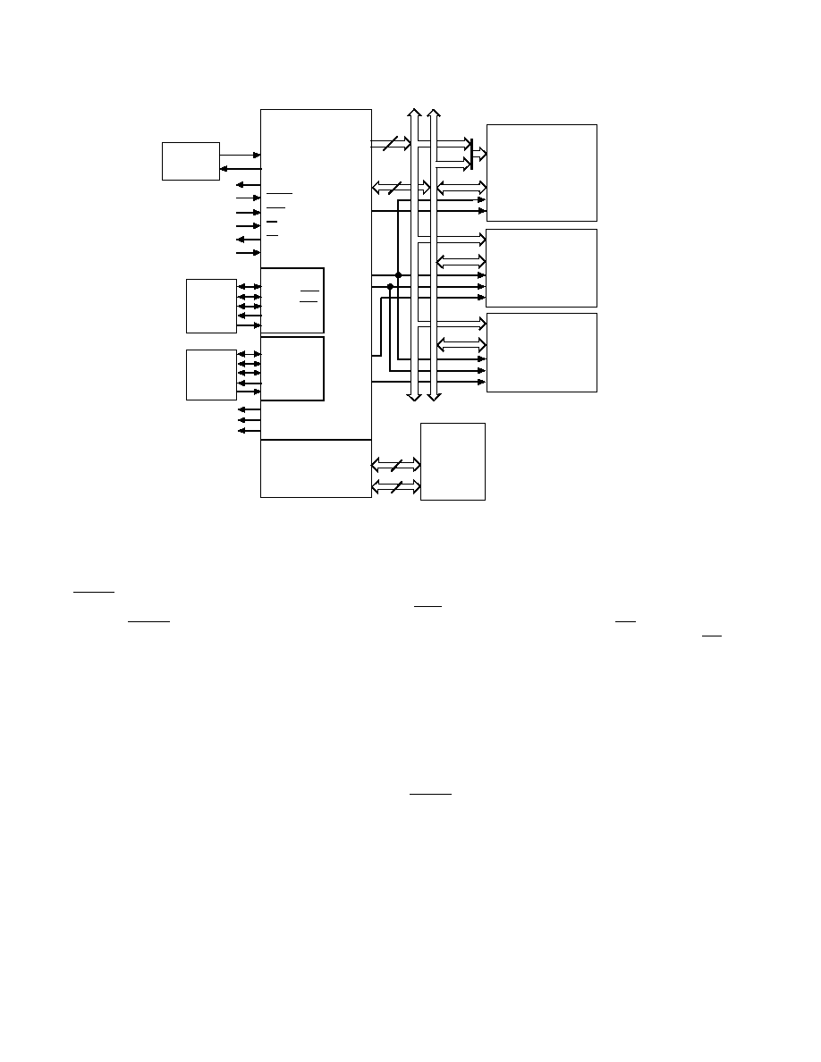
Figure 5. ADSP-2111 System
The RESET input resets all internal stack pointers to the empty
stack condition, masks all interrupts, and clears the MSTAT
register. When RESET is released, the boot loading sequence is
performed (provided there is no pending bus request and the
chip is configured for booting, with MMAP = 0). The first
instruction is then fetched from internal program memory
location 0x0000.
Program Memory Interface
The on-chip program memory address bus (PMA) and on-chip
program memory data bus (PMD) are multiplexed with the on-
chip data memory buses (DMA, DMD), creating a single
external data bus and a single external address bus. The external
data bus is bidirectional and is 24 bits wide to allow instruction
fetches from external program memory. Program memory may
contain code and data.
The external address bus is 14 bits wide. For the ADSP-2101,
ADSP-2103, and ADSP-2111, these lines can directly address
up to 16K words, of which 2K are on-chip. For the ADSP-2105
and ADSP-2115, the address lines can directly address up to
15K words, of which 1K is on-chip.
The data lines are bidirectional. The program memory select
(PMS) signal indicates accesses to program memory and can be
used as a chip select signal. The write (WR) signal indicates a
write operation and is used as a write strobe. The read (RD)
signal indicates a read operation and is used as a read strobe or
output enable signal.
The ADSP-21xx processors write data from their 16-bit
registers to 24-bit program memory using the PX register to
provide the lower eight bits. When the processor reads 16-bit
data from 24-bit program memory to a 16-bit data register, the
lower eight bits are placed in the PX register.
The program memory interface can generate 0 to 7 wait states
for external memory devices; default is to 7 wait states after
RESET
.
Program Memory Maps
Program memory can be mapped in two ways, depending on the
state of the MMAP pin. Figure 6 shows the two program
memory maps for the ADSP-2101, ADSP-2103, and
ADSP-2111. Figure 8 shows the program memory maps for the
ADSP-2105 and ADSP-2115. Figures 7 and 9 show the
program memory maps for the ADSP-2161/62 and ADSP-2163/
64, respectively.
BR
BG
CLKIN
RESET
IRQ2
BMS
CLKOUT
ADDR
DATA
(OPTIONAL)
1x CLOCK
or
CRYSTAL
PMS
DMS
RD
WR
ADDR
13-0
DATA
23-0
ADDR
DATA
(OPTIONAL)
ADDR
DATA
BOOT
MEMORY
e.g. EPROM
2764
27128
27256
27512
PROGRAM
MEMORY
DATA
MEMORY
&
PERIPHERALS
14
24
D
23-22
A
13-0
D
15-8
D
23-0
D
23-8
A
13-0
A
13-0
XTAL
MMAP
SERIAL
DEVICE
(OPTIONAL)
SCLK1
RFS1
or IRQ0
TFS1
or IRQ1
DT1
or FO
DR1
or FI
SPORT 1
SCLK0
RFS0
TFS0
DT0
DR0
SPORT 0
SERIAL
DEVICE
(OPTIONAL)
OE
WE
CS
OE
WE
CS
OE
CS
ADSP-2111
HOST
PROCESSOR
(OPTIONAL)
HOST INTERFACE PORT
CONTROL
DATA / ADDR
(OPTIONAL)
FL0
FL1
FL2
7
16
THE TWO MSBs OF THE DATA BUS (D
23-22
) ARE USED TO SUPPLY THE TWO MSBs OF THE
BOOT MEMORY EPROM ADDRESS. THIS IS ONLY REQUIRED FOR THE 27256 AND 27512.
相关PDF资料 |
PDF描述 |
|---|---|
| VI-B2Z-CX-F4 | CONVERTER MOD DC/DC 2V 30W |
| DSEP30-06BR | DIODE 600V 30A ISOPLUS247 |
| TAJY107M016Y | CAP TANT 100UF 16V 20% 2917 |
| VI-B2Z-CW-F3 | CONVERTER MOD DC/DC 2V 40W |
| ADSP-21061LKB-160 | IC DSP CONTROLLER 32BIT 225BGA |
相关代理商/技术参数 |
参数描述 |
|---|---|
| ADSP-2101BG-40 | 制造商:Rochester Electronics LLC 功能描述:- Bulk |
| ADSP-2101BG-50 | 制造商:Analog Devices 功能描述: |
| ADSP-2101BG-66 | 制造商:AD 制造商全称:Analog Devices 功能描述:ADSP-2100 Family DSP Microcomputers |
| ADSP-2101BG-80 | 制造商:AD 制造商全称:Analog Devices 功能描述:ADSP-2100 Family DSP Microcomputers |
| ADSP-2101BGZ-100 | 制造商:Analog Devices 功能描述:DSP FIX PT 16BIT 25MHZ 25MIPS 68CPGA - Trays |
发布紧急采购,3分钟左右您将得到回复。