- 您现在的位置:买卖IC网 > PDF目录19369 > ADSP-21060LCB-133 (Analog Devices Inc)IC DSP CONTROLLER 32BIT 225BGA PDF资料下载
参数资料
| 型号: | ADSP-21060LCB-133 |
| 厂商: | Analog Devices Inc |
| 文件页数: | 2/64页 |
| 文件大小: | 0K |
| 描述: | IC DSP CONTROLLER 32BIT 225BGA |
| 产品培训模块: | SHARC Processor Overview |
| 标准包装: | 1 |
| 系列: | SHARC® |
| 类型: | 浮点 |
| 接口: | 主机接口,连接端口,串行端口 |
| 时钟速率: | 33MHz |
| 非易失内存: | 外部 |
| 芯片上RAM: | 512kB |
| 电压 - 输入/输出: | 3.30V |
| 电压 - 核心: | 3.30V |
| 工作温度: | -40°C ~ 100°C |
| 安装类型: | 表面贴装 |
| 封装/外壳: | 225-BBGA |
| 供应商设备封装: | 225-PBGA |
| 包装: | 托盘 |
第1页当前第2页第3页第4页第5页第6页第7页第8页第9页第10页第11页第12页第13页第14页第15页第16页第17页第18页第19页第20页第21页第22页第23页第24页第25页第26页第27页第28页第29页第30页第31页第32页第33页第34页第35页第36页第37页第38页第39页第40页第41页第42页第43页第44页第45页第46页第47页第48页第49页第50页第51页第52页第53页第54页第55页第56页第57页第58页第59页第60页第61页第62页第63页第64页
Rev. F
|
Page 10 of 64
|
March 2008
ADSP-21060/ADSP-21060L/ADSP-21062/ADSP-21062L/ADSP-21060C/ADSP-21060LC
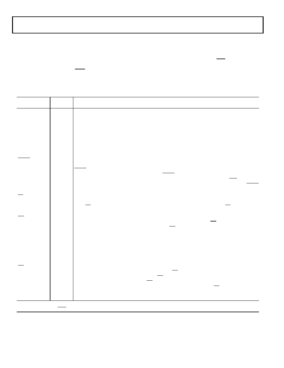
PIN FUNCTION DESCRIPTIONS
The ADSP-2106x pin definitions are listed below. Inputs identi-
fied as synchronous (S) must meet timing requirements with
respect to CLKIN (or with respect to TCK for TMS, TDI).
Inputs identified as asynchronous (A) can be asserted asynchro-
nously to CLKIN (or to TCK for TRST).
Unused inputs should be tied or pulled to VDD or GND, except
for ADDR31–0, DATA47–0, FLAG3–0, and inputs that have
internal pull-up or pull-down resistors (CPA, ACK, DTx, DRx,
TCLKx, RCLKx, LxDAT3–0, LxCLK, LxACK, TMS, and
TDI)—these pins can be left floating. These pins have a
logic-level hold circuit that prevents the input from floating
internally.
Table 3. Pin Descriptions
Pin
Type
Function
ADDR31–0
I/O/T
External Bus Address. The ADSP-2106x outputs addresses for external memory and peripherals on these
pins. In a multiprocessor system, the bus master outputs addresses for read/write of the internal memory
or IOP registers of other ADSP-2106xs. The ADSP-2106x inputs addresses when a host processor or multi-
processing bus master is reading or writing its internal memory or IOP registers.
DATA47–0
I/O/T
External Bus Data. The ADSP-2106x inputs and outputs data and instructions on these pins. 32-bit single-
precision floating-point data and 32-bit fixed-point data is transferred over bits 47–16 of the bus. 40-bit
extended-precision floating-point data is transferred over bits 47–8 of the bus. 16-bit short word data is
transferred over bits 31–16 of the bus. In PROM boot mode, 8-bit data is transferred over bits 23–16. Pull-up
resistors on unused DATA pins are not necessary.
MS3–0
O/T
Memory Select Lines. These lines are asserted (low) as chip selects for the corresponding banks of external
memory. Memory bank size must be defined in the ADSP-2106x’s system control register (SYSCON). The
MS3–0 lines are decoded memory address lines that change at the same time as the other address lines.
When no external memory access is occurring, the MS3–0 lines are inactive; they are active however when
a conditional memory access instruction is executed, whether or not the condition is true. MS0 can be used
with the PAGE signal to implement a bank of DRAM memory (Bank 0). In a multiprocessing system the MS3–0
lines are output by the bus master.
RD
I/O/T
Memory Read Strobe. This pin is asserted (low) when the ADSP-2106x reads from external memory devices
or from the internal memory of other ADSP-2106xs. External devices (including other ADSP-2106xs) must
assert RD to read from the ADSP-2106x’s internal memory. In a multiprocessing system, RD is output by the
bus master and is input by all other ADSP-2106xs.
WR
I/O/T
Memory Write Strobe. This pin is asserted (low) when the ADSP-2106x writes to external memory devices
or to the internal memory of other ADSP-2106xs. External devices must assert WR to write to the ADSP-
2106x’s internal memory. In a multiprocessing system, WR is output by the bus master and is input by all
other ADSP-2106xs.
PAGE
O/T
DRAM Page Boundary. The ADSP-2106x asserts this pin to signal that an external DRAM page boundary
has been crossed. DRAM page size must be defined in the ADSP-2106x’s memory control register (WAIT).
DRAM can only be implemented in external memory Bank 0; the PAGE signal can only be activated for Bank
0 accesses. In a multiprocessing system, PAGE is output by the bus master
ADRCLK
O/T
Clock Output Reference. In a multiprocessing system, ADRCLK is output by the bus master.
SW
I/O/T
Synchronous Write Select. This signal is used to interface the ADSP-2106x to synchronous memory devices
(including other ADSP-2106xs). The ADSP-2106x asserts SW (low) to provide an early indication of an
impending write cycle, which can be aborted if WR is not later asserted (e.g., in a conditional write
instruction). In a multiprocessing system, SW is output by the bus master and is input by all other
ADSP-2106xs to determine if the multiprocessor memory access is a read or write. SW is asserted at the same
time as the address output. A host processor using synchronous writes must assert this pin when writing to
the ADSP-2106x(s).
A = Asynchronous, G = Ground, I = Input, O = Output, P = Power Supply, S = Synchronous, (A/D) = Active Drive, (O/D) = Open Drain,
T = Three-State (when SBTS is asserted, or when the ADSP-2106x is a bus slave)
相关PDF资料 |
PDF描述 |
|---|---|
| VI-B4Z-CY-F2 | CONVERTER MOD DC/DC 2V 20W |
| ATFC-0402-1N2-BT | INDUCTOR THIN FILM 1.2NH 0402 |
| ADSP-21060LAB-160 | IC DSP CONTROLLER 32BIT 225BGA |
| REC3-1215DRW/H/B | CONV DC/DC 3W 9-18VIN +/-15VOUT |
| TAJY107K016A | CAP TANT 100UF 16V 10% 2917 |
相关代理商/技术参数 |
参数描述 |
|---|---|
| ADSP-21060LCBZ-133 | 功能描述:IC DSP CONTROLLER 32BIT 225PBGA RoHS:是 类别:集成电路 (IC) >> 嵌入式 - DSP(数字式信号处理器) 系列:SHARC® 标准包装:2 系列:StarCore 类型:SC140 内核 接口:DSI,以太网,RS-232 时钟速率:400MHz 非易失内存:外部 芯片上RAM:1.436MB 电压 - 输入/输出:3.30V 电压 - 核心:1.20V 工作温度:-40°C ~ 105°C 安装类型:表面贴装 封装/外壳:431-BFBGA,FCBGA 供应商设备封装:431-FCPBGA(20x20) 包装:托盘 |
| ADSP-21060LCW-133 | 制造商:Analog Devices 功能描述:DSP Floating-Point 32-Bit 33MHz 33MIPS 240-Pin CQFP 制造商:Rochester Electronics LLC 功能描述:SHARC IND.,3V,33MHZ CQFP HEAT SLUG DOWN - Bulk |
| ADSP-21060LCW-160 | 功能描述:IC DSP CONTROLLER 32BIT 240CQFP RoHS:否 类别:集成电路 (IC) >> 嵌入式 - DSP(数字式信号处理器) 系列:SHARC® 标准包装:2 系列:StarCore 类型:SC140 内核 接口:DSI,以太网,RS-232 时钟速率:400MHz 非易失内存:外部 芯片上RAM:1.436MB 电压 - 输入/输出:3.30V 电压 - 核心:1.20V 工作温度:-40°C ~ 105°C 安装类型:表面贴装 封装/外壳:431-BFBGA,FCBGA 供应商设备封装:431-FCPBGA(20x20) 包装:托盘 |
| ADSP-21060LCWZ-133 | 制造商:Analog Devices 功能描述:SHARC INDUSTRIAL 5V CQFP HEAT SLUG UP - Trays |
| ADSP-21060LCWZ-160 | 制造商:Analog Devices 功能描述:DSP Floating-Point 32-Bit 40MHz 40MIPS 240-Pin CQFP 制造商:Analog Devices 功能描述:DSP FLOATING PT 32BIT 40MHZ 40MIPS 240CQFP - Trays 制造商:Analog Devices 功能描述:IC DSP SHARC 32BIT 40MHZ CQFP240 |
发布紧急采购,3分钟左右您将得到回复。