- 您现在的位置:买卖IC网 > PDF目录19376 > ADSP-21061KS-160 (Analog Devices Inc)IC DSP CONTROLLER 1MBIT 240MQFP PDF资料下载
参数资料
| 型号: | ADSP-21061KS-160 |
| 厂商: | Analog Devices Inc |
| 文件页数: | 38/52页 |
| 文件大小: | 0K |
| 描述: | IC DSP CONTROLLER 1MBIT 240MQFP |
| 产品培训模块: | SHARC Processor Overview |
| 标准包装: | 1 |
| 系列: | SHARC® |
| 类型: | 浮点 |
| 接口: | 同步串行端口(SSP) |
| 时钟速率: | 40MHz |
| 非易失内存: | 外部 |
| 芯片上RAM: | 128kB |
| 电压 - 输入/输出: | 5.00V |
| 电压 - 核心: | 5.00V |
| 工作温度: | 0°C ~ 85°C |
| 安装类型: | 表面贴装 |
| 封装/外壳: | 240-BFQFP 裸露焊盘 |
| 供应商设备封装: | 240-MQFP-EP(32x32) |
| 包装: | 托盘 |
第1页第2页第3页第4页第5页第6页第7页第8页第9页第10页第11页第12页第13页第14页第15页第16页第17页第18页第19页第20页第21页第22页第23页第24页第25页第26页第27页第28页第29页第30页第31页第32页第33页第34页第35页第36页第37页当前第38页第39页第40页第41页第42页第43页第44页第45页第46页第47页第48页第49页第50页第51页第52页
Rev. D | Page 43 of 52 | May 2013
TEST CONDITIONS
Output Disable Time
Output pins are considered to be disabled when they stop driv-
ing, go into a high impedance state, and start to decay from their
output high or low voltage. The time for the voltage on the bus
to decay by V is dependent on the capacitive load, CL, and the
load current, IL. This decay time can be approximated by the
following equation:
The output disable time tDIS is the difference between
the interval from when the reference signal switches to when the
output voltage decays V from the measured output high or
output low voltage. tDECAY is calculated with test loads CL and IL,
and with V equal to 0.5 V.
Output Enable Time
Output pins are considered to be enabled when they have made
a transition from a high impedance state to when they start driv-
ing. The output enable time tENA is the interval from when a
reference signal reaches a high or low voltage level to when the
output has reached a specified high or low trip point, as shown
in the Output Enable/Disable diagram (Figure 27). If multiple
pins (such as the data bus) are enabled, the measurement value
is that of the first pin to start driving.
Example System Hold Time Calculation
To determine the data output hold time in a particular system,
first calculate tDECAY using the equation given above. Choose V
to be the difference between the ADSP-21061’s output voltage
and the input threshold for the device requiring the hold time. A
typical V will be 0.4 V. CL is the total bus capacitance (per data
line), and IL is the total leakage or three-state current (per data
line). The hold time will be tDECAY plus the minimum disable
time (i.e., tDATRWH for the write cycle).
Output Drive Characteristics
output drivers of the ADSP-21061 (5 V) and ADSP-21061L
(3 V). The curves represent the current drive capability and
switching behavior of the output drivers as a function of
resistive and capacitive loading.
Capacitive Loading
Output delays and holds are based on standard capacitive loads:
50 pF on all pins (see Figure 28). The delay and hold specifica-
tions given should be derated by a factor of 1.5 ns/50 pF for
loads other than the nominal value of 50 pF. Figure 31,
cally how output delays and holds vary with load capacitance.
(Note that this graph or derating does not apply to output dis-
able delays; see the previous section Output Disable Time under
Test Conditions.) The graphs of Figure 31, Figure 32, Figure 35,
and Figure 36 may not be linear outside the ranges shown.
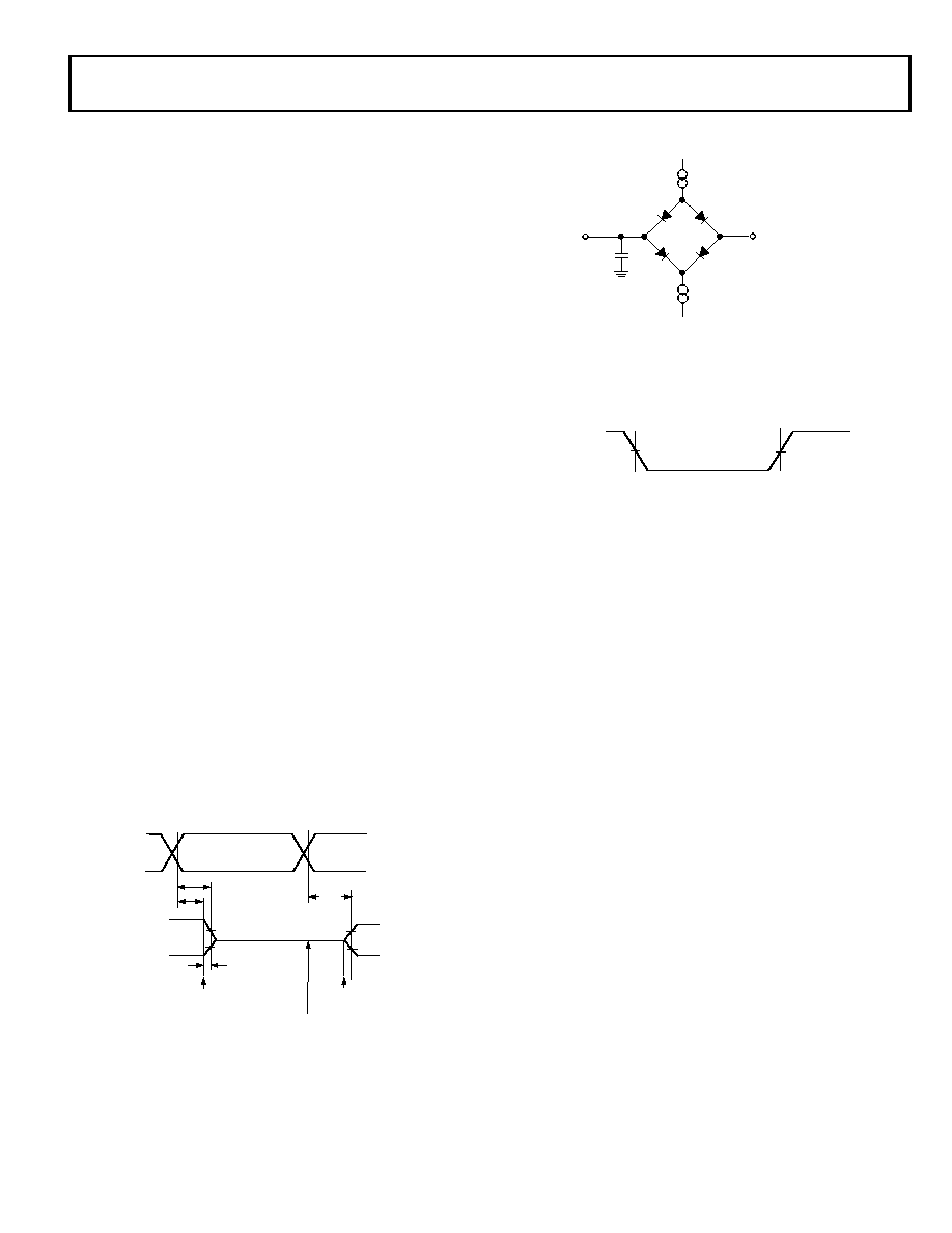
Figure 27. Output Enable/Disable
PEXT
CL V
IL
---------------
=
REFERENCE
SIGNAL
tDIS
OUTPUT STARTS
DRIVING
VOH (MEASURED) - V
VOL (MEASURED) + V
tMEASURED
VOH (MEASURED)
VOL (MEASURED)
2.0V
1.0V
VOH (MEASURED)
VOL (MEASURED)
HIGH IMPEDANCE STATE.
TESTCONDITIONS CAUSE
THIS VOLTAGE TO BE
APPROXIMATELY 1.5V.
OUTPUT STOPS
DRIVING
tENA
tDECAY
Figure 28. Equivalent Device Loading for AC Measurements (Includes All
Fixtures)
Figure 29. Voltage Reference Levels for AC Measurements (Except Output
Enable/Disable)
1.5V
50pF
TO
OUTPUT
PIN
IOL
IOH
INPUT
OR
OUTPUT
1.5V
相关PDF资料 |
PDF描述 |
|---|---|
| MAX6665ASA40+T | IC FAN CNTRL/DRVR 8-SOIC |
| VI-B3B-CY-F4 | CONVERTER MOD DC/DC 95V 50W |
| MAX6665ASA50+T | IC FAN CNTRL/DRVR 8-SOIC |
| VI-B34-CY-F1 | CONVERTER MOD DC/DC 48V 50W |
| 5718-RC | CHOKE RF HI CURR 1100UH 15% RAD |
相关代理商/技术参数 |
参数描述 |
|---|---|
| ADSP-21061KS-200 | 功能描述:IC DSP CONTROLLER 32BIT 240MQFP RoHS:否 类别:集成电路 (IC) >> 嵌入式 - DSP(数字式信号处理器) 系列:SHARC® 标准包装:2 系列:StarCore 类型:SC140 内核 接口:DSI,以太网,RS-232 时钟速率:400MHz 非易失内存:外部 芯片上RAM:1.436MB 电压 - 输入/输出:3.30V 电压 - 核心:1.20V 工作温度:-40°C ~ 105°C 安装类型:表面贴装 封装/外壳:431-BFBGA,FCBGA 供应商设备封装:431-FCPBGA(20x20) 包装:托盘 |
| ADSP-21061KS-200X | 制造商:未知厂家 制造商全称:未知厂家 功能描述:32-Bit Digital Signal Processor |
| ADSP-21061KSZ-133 | 功能描述:IC DSP CONTROLLER 32BIT 240MQFP RoHS:是 类别:集成电路 (IC) >> 嵌入式 - DSP(数字式信号处理器) 系列:SHARC® 标准包装:2 系列:StarCore 类型:SC140 内核 接口:DSI,以太网,RS-232 时钟速率:400MHz 非易失内存:外部 芯片上RAM:1.436MB 电压 - 输入/输出:3.30V 电压 - 核心:1.20V 工作温度:-40°C ~ 105°C 安装类型:表面贴装 封装/外壳:431-BFBGA,FCBGA 供应商设备封装:431-FCPBGA(20x20) 包装:托盘 |
| ADSP-21061KSZ-160 | 功能描述:IC DSP CONTROLLER 1MBIT 240MQFP RoHS:是 类别:集成电路 (IC) >> 嵌入式 - DSP(数字式信号处理器) 系列:SHARC® 标准包装:40 系列:TMS320DM64x, DaVinci™ 类型:定点 接口:I²C,McASP,McBSP 时钟速率:400MHz 非易失内存:外部 芯片上RAM:160kB 电压 - 输入/输出:3.30V 电压 - 核心:1.20V 工作温度:0°C ~ 90°C 安装类型:表面贴装 封装/外壳:548-BBGA,FCBGA 供应商设备封装:548-FCBGA(27x27) 包装:托盘 配用:TMDSDMK642-0E-ND - DEVELPER KIT W/NTSC CAMERA296-23038-ND - DSP STARTER KIT FOR TMS320C6416296-23059-ND - FLASHBURN PORTING KIT296-23058-ND - EVAL MODULE FOR DM642TMDSDMK642-ND - DEVELOPER KIT W/NTSC CAMERA |
| ADSP-21061KSZ-200 | 功能描述:IC DSP CONTROLLER 32BIT 240MQFP RoHS:是 类别:集成电路 (IC) >> 嵌入式 - DSP(数字式信号处理器) 系列:SHARC® 标准包装:40 系列:TMS320DM64x, DaVinci™ 类型:定点 接口:I²C,McASP,McBSP 时钟速率:400MHz 非易失内存:外部 芯片上RAM:160kB 电压 - 输入/输出:3.30V 电压 - 核心:1.20V 工作温度:0°C ~ 90°C 安装类型:表面贴装 封装/外壳:548-BBGA,FCBGA 供应商设备封装:548-FCBGA(27x27) 包装:托盘 配用:TMDSDMK642-0E-ND - DEVELPER KIT W/NTSC CAMERA296-23038-ND - DSP STARTER KIT FOR TMS320C6416296-23059-ND - FLASHBURN PORTING KIT296-23058-ND - EVAL MODULE FOR DM642TMDSDMK642-ND - DEVELOPER KIT W/NTSC CAMERA |
发布紧急采购,3分钟左右您将得到回复。