- 您现在的位置:买卖IC网 > PDF目录19401 > ADSP-21478BCPZ-1A (Analog Devices Inc)IC DSP SHARK 200MHZ 88LFCSP PDF资料下载
参数资料
| 型号: | ADSP-21478BCPZ-1A |
| 厂商: | Analog Devices Inc |
| 文件页数: | 9/76页 |
| 文件大小: | 0K |
| 描述: | IC DSP SHARK 200MHZ 88LFCSP |
| 标准包装: | 1 |
| 系列: | SHARC® |
| 类型: | 浮点 |
| 接口: | DAI,DPI,EBI/EMI,I²C,SPI,SPORT,UART/USART |
| 时钟速率: | 200MHz |
| 非易失内存: | ROM(4Mb) |
| 芯片上RAM: | 3Mb |
| 电压 - 输入/输出: | 3.30V |
| 电压 - 核心: | 1.20V |
| 工作温度: | -40°C ~ 85°C |
| 安装类型: | 表面贴装 |
| 封装/外壳: | 88-VFQFN 裸露焊盘,CSP |
| 供应商设备封装: | 88-LFCSP-VQ(12x12) |
| 包装: | 托盘 |
第1页第2页第3页第4页第5页第6页第7页第8页当前第9页第10页第11页第12页第13页第14页第15页第16页第17页第18页第19页第20页第21页第22页第23页第24页第25页第26页第27页第28页第29页第30页第31页第32页第33页第34页第35页第36页第37页第38页第39页第40页第41页第42页第43页第44页第45页第46页第47页第48页第49页第50页第51页第52页第53页第54页第55页第56页第57页第58页第59页第60页第61页第62页第63页第64页第65页第66页第67页第68页第69页第70页第71页第72页第73页第74页第75页第76页
Rev. C
|
Page 17 of 76
|
July 2013
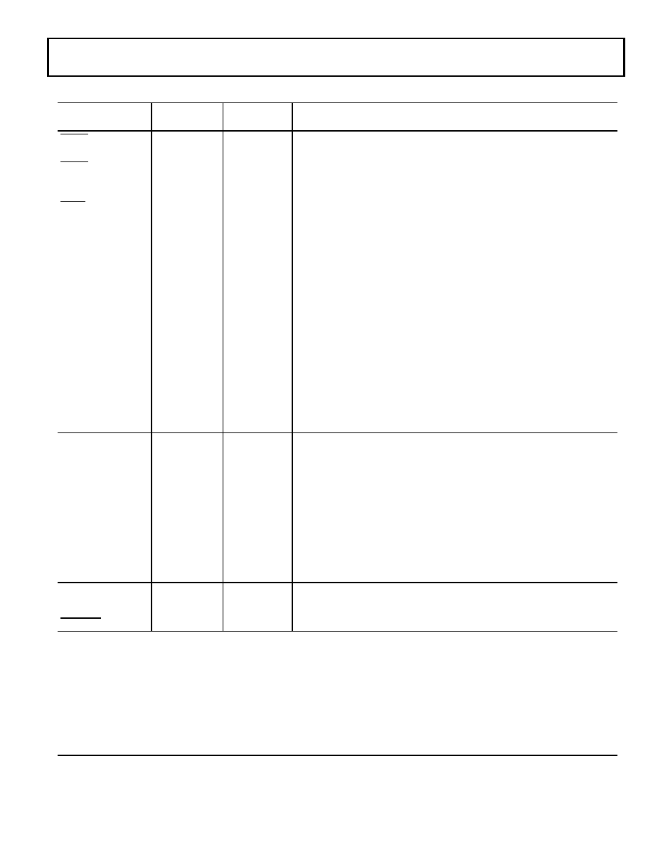
SDRAS
O/T (ipu)
High-Z/
driven high
SDRAM Row Address Strobe. Connect to SDRAM’s RAS pin. In conjunction with
other SDRAM command pins, defines the operation for the SDRAM to perform.
SDCAS
O/T (ipu)
High-Z/
driven high
SDRAM Column Address Select. Connect to SDRAM’s CAS pin. In conjunction
with other SDRAM command pins, defines the operation for the SDRAM to
perform.
SDWE
O/T (ipu)
High-Z/
driven high
SDRAM Write Enable. Connect to SDRAM’s WE or W buffer pin.
SDCKE
O/T (ipu)
High-Z/
driven high
SDRAM Clock Enable. Connect to SDRAM’s CKE pin. Enables and disables the CLK
signal. For details, see the data sheet supplied with the SDRAM device.
SDA10
O/T (ipu)
High-Z/
driven high
SDRAM A10 Pin. Enables applications to refresh an SDRAM in parallel with non-
SDRAM accesses. This pin replaces the DSP’s ADDR10 pin only during SDRAM
accesses.
SDDQM
O/T (ipu)
High-Z/
driven high
DQM Data Mask. SDRAM input mask signal for write accesses and output enable
signal for read accesses. Input data is masked when DQM is sampled high during
a write cycle. The SDRAM output buffers are placed in a High-Z state when DQM
is sampled high during a read cycle. SDDQM is driven high from reset de-assertion
until SDRAM initialization completes. Afterwards, it is driven low irrespective of
whether any SDRAM accesses occur or not.
SDCLK
O/T (ipd)
High-Z/
driving
SDRAM Clock Output. Clock driver for this pin differs from all other clock drivers.
See Figure 47 on Page 65. For models in the 100-lead package, the SDRAM
interface should be disabled to avoid unnecessary power switching by setting the
DSDCTL bit in SDCTL register. For more information, see the ADSP-214xx SHARC
Processor Hardware Reference.
DAI _P20–1
I/O/T (ipu)
High-Z
Digital Applications Interface. These pins provide the physical interface to the
DAI SRU. The DAI SRU configuration registers define the combination of on-chip
audio-centric peripheral inputs or outputs connected to the pin and to the pin’s
output enable. The configuration registers of these peripherals then determines
the exact behavior of the pin. Any input or output signal present in the DAI SRU
may be routed to any of these pins.
DPI _P14–1
I/O/T (ipu)
High-Z
Digital Peripheral Interface. These pins provide the physical interface to the DPI
SRU. The DPI SRU configuration registers define the combination of on-chip
peripheral inputs or outputs connected to the pin and to the pin's output enable.
The configuration registers of these peripherals then determine the exact
behavior of the pin. Any input or output signal present in the DPI SRU may be
routed to any of these pins.
WDT_CLKIN
I
Watch Dog Timer Clock Input. This pin should be pulled low when not used.
WDT_CLKO
O
Watch Dog Resonator Pad Output.
WDTRSTO
O (ipu)
Watch Dog Timer Reset Out.
Table 11. Pin Descriptions (Continued)
Name
Type
State During/
After Reset
Description
The following symbols appear in the Type column of Table 11: A = asynchronous, I =input, O = output, S = synchronous, A/D = active drive,
O/D = open drain, and T = three-state, ipd = internal pull-down resistor, ipu = internal pull-up resistor.
The internal pull-up (ipu) and internal pull-down (ipd) resistors are designed to hold the internal path from the pins at the expected logic
levels. To pull-up or pull-down the external pads to the expected logic levels, use external resistors. Internal pull-up/pull-down resistors
cannot be enabled/disabled and the value of these resistors cannot be programmed. The range of an ipu resistor can be 26 kΩ to 63 kΩ. The
range of an ipd resistor can be 31 kΩ to 85 kΩ. The three-state voltage of ipu pads will not reach to full the VDD_EXT level; at typical conditions
the voltage is in the range of 2.3 V to 2.7 V.
In this table, all pins are LVTTL compliant with the exception of the thermal diode, shift register, and real-time clock (RTC) pins.
Not all pins are available in the 88-lead LFCSP_VQ and 100-lead LQFP package. For more information, see Table 2 on Page 3 and Table 62 on
Page 70.
相关PDF资料 |
PDF描述 |
|---|---|
| 5704-RC | CHOKE RF HI CURR 275UH 15% RAD |
| VI-22X-CY-F3 | CONVERTER MOD DC/DC 5.2V 50W |
| VI-22W-CY-F1 | CONVERTER MOD DC/DC 5.5V 50W |
| 5711-RC | CHOKE RF HI CURRENT 50UH 15% RAD |
| ADSP-21479KCPZ-1A | IC DSP SHARK 200MHZ 88LFCSP |
相关代理商/技术参数 |
参数描述 |
|---|---|
| ADSP-21478BSWZ-2A | 功能描述:IC DSP SHARC 266MHZ LP 100LQFP RoHS:是 类别:集成电路 (IC) >> 嵌入式 - DSP(数字式信号处理器) 系列:SHARC® 标准包装:40 系列:TMS320DM64x, DaVinci™ 类型:定点 接口:I²C,McASP,McBSP 时钟速率:400MHz 非易失内存:外部 芯片上RAM:160kB 电压 - 输入/输出:3.30V 电压 - 核心:1.20V 工作温度:0°C ~ 90°C 安装类型:表面贴装 封装/外壳:548-BBGA,FCBGA 供应商设备封装:548-FCBGA(27x27) 包装:托盘 配用:TMDSDMK642-0E-ND - DEVELPER KIT W/NTSC CAMERA296-23038-ND - DSP STARTER KIT FOR TMS320C6416296-23059-ND - FLASHBURN PORTING KIT296-23058-ND - EVAL MODULE FOR DM642TMDSDMK642-ND - DEVELOPER KIT W/NTSC CAMERA |
| ADSP-21478BSWZ-2AX | 制造商:Analog Devices 功能描述:- Trays |
| ADSP-21478KBCZ-1A | 功能描述:IC DSP SHARC 200MHZ LP 196CSPBGA RoHS:是 类别:集成电路 (IC) >> 嵌入式 - DSP(数字式信号处理器) 系列:SHARC® 标准包装:2 系列:StarCore 类型:SC140 内核 接口:DSI,以太网,RS-232 时钟速率:400MHz 非易失内存:外部 芯片上RAM:1.436MB 电压 - 输入/输出:3.30V 电压 - 核心:1.20V 工作温度:-40°C ~ 105°C 安装类型:表面贴装 封装/外壳:431-BFBGA,FCBGA 供应商设备封装:431-FCPBGA(20x20) 包装:托盘 |
| ADSP-21478KBCZ-2A | 功能描述:IC DSP SHARK 266MHZ 196CSPBGA RoHS:是 类别:集成电路 (IC) >> 嵌入式 - DSP(数字式信号处理器) 系列:SHARC® 标准包装:2 系列:StarCore 类型:SC140 内核 接口:DSI,以太网,RS-232 时钟速率:400MHz 非易失内存:外部 芯片上RAM:1.436MB 电压 - 输入/输出:3.30V 电压 - 核心:1.20V 工作温度:-40°C ~ 105°C 安装类型:表面贴装 封装/外壳:431-BFBGA,FCBGA 供应商设备封装:431-FCPBGA(20x20) 包装:托盘 |
| ADSP-21478KBCZ-3A | 功能描述:IC DSP SHARK 300MHZ 196CSPBGA RoHS:是 类别:集成电路 (IC) >> 嵌入式 - DSP(数字式信号处理器) 系列:SHARC® 标准包装:2 系列:StarCore 类型:SC140 内核 接口:DSI,以太网,RS-232 时钟速率:400MHz 非易失内存:外部 芯片上RAM:1.436MB 电压 - 输入/输出:3.30V 电压 - 核心:1.20V 工作温度:-40°C ~ 105°C 安装类型:表面贴装 封装/外壳:431-BFBGA,FCBGA 供应商设备封装:431-FCPBGA(20x20) 包装:托盘 |
发布紧急采购,3分钟左右您将得到回复。