- 您现在的位置:买卖IC网 > PDF目录19483 > ADSP-21479BSWZ-2A (Analog Devices Inc)IC DSP SHARC 266MHZ LP 100LQFP PDF资料下载
参数资料
| 型号: | ADSP-21479BSWZ-2A |
| 厂商: | Analog Devices Inc |
| 文件页数: | 56/72页 |
| 文件大小: | 0K |
| 描述: | IC DSP SHARC 266MHZ LP 100LQFP |
| 标准包装: | 1 |
| 系列: | SHARC® |
| 类型: | 浮点 |
| 接口: | DAI,DPI,EBI/EMI,I²C,SPI,SPORT,UART/USART |
| 时钟速率: | 266MHz |
| 非易失内存: | ROM(4Mb) |
| 芯片上RAM: | 5Mb |
| 电压 - 输入/输出: | 3.30V |
| 电压 - 核心: | 1.20V |
| 工作温度: | -40°C ~ 85°C |
| 安装类型: | 表面贴装 |
| 封装/外壳: | 100-LQFP 裸露焊盘 |
| 供应商设备封装: | 100-LQFP-EP(14x14) |
| 包装: | 托盘 |
第1页第2页第3页第4页第5页第6页第7页第8页第9页第10页第11页第12页第13页第14页第15页第16页第17页第18页第19页第20页第21页第22页第23页第24页第25页第26页第27页第28页第29页第30页第31页第32页第33页第34页第35页第36页第37页第38页第39页第40页第41页第42页第43页第44页第45页第46页第47页第48页第49页第50页第51页第52页第53页第54页第55页当前第56页第57页第58页第59页第60页第61页第62页第63页第64页第65页第66页第67页第68页第69页第70页第71页第72页
Rev. A
|
Page 6 of 72
|
September 2011
The processor’s SRAM can be configured as a maximum of
160k words of 32-bit data, 320k words of 16-bit data, 106.7k
words of 48-bit instructions (or 40-bit data), or combinations of
different word sizes up to 5 megabits. All of the memory can be
accessed as 16-bit, 32-bit, 48-bit, or 64-bit words. A 16-bit
floating-point storage format is supported that effectively dou-
bles the amount of data that may be stored on-chip. Conversion
between the 32-bit floating-point and 16-bit floating-point
formats is performed in a single instruction. While each mem-
ory block can store combinations of code and data, accesses are
most efficient when one block stores data using the DM bus for
transfers, and the other block stores instructions and data using
the PM bus for transfers.
Using the DM bus and PM buses, with one bus dedicated to a
memory block, assures single-cycle execution with two data
transfers. In this case, the instruction must be available in the
cache.
memory address space of the processors. The 48-bit space sec-
tion describes what this address range looks like to an
instruction that retrieves 48-bit memory. The 32-bit section
describes what this address range looks like to an instruction
that retrieves 32-bit memory.
On-Chip Memory Bandwidth
The internal memory architecture allows programs to have four
accesses at the same time to any of the four blocks (assuming
there are no block conflicts). The total bandwidth is realized
using the DMD and PMD buses (2 × 64-bits at CCLK speed)
and the IOD0/1 buses (2 × 32-bit at PCLK speed).
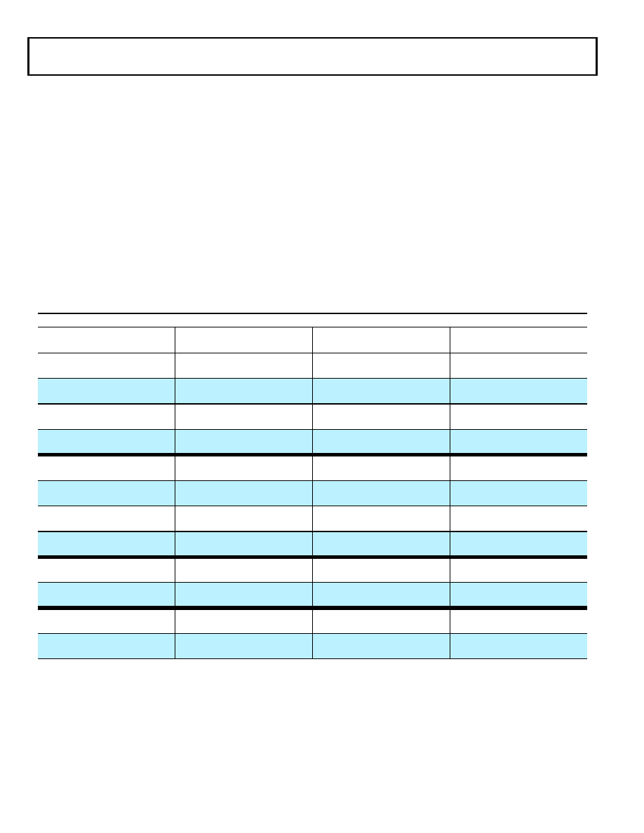
Table 3. ADSP-21478 Internal Memory Space (3 Mbit)1
IOP Registers 0x0000 0000–0x0003 FFFF
Long Word (64 Bits)
Extended Precision Normal or
Instruction Word (48 Bits)
Normal Word (32 Bits)
Short Word (16 Bits)
Block 0 ROM (Reserved)
0x0004 0000–0x0004 7FFF
Block 0 ROM (Reserved)
0x0008 0000–0x0008 AAA9
Block 0 ROM (Reserved)
0x0008 0000–0x0008 FFFF
Block 0 ROM (Reserved)
0x0010 0000–0x0011 FFFF
Reserved
0x0004 8000–0x0004 8FFF
Reserved
0x0008 AAAA–0x0008 BFFF
Reserved
0x0009 0000–0x0009 1FFF
Reserved
0x0012 0000–0x0012 3FFF
Block 0 SRAM
0x0004 9000–0x0004 CFFF
Block 0 SRAM
0x0008 C000–0x0009 1554
Block 0 SRAM
0x0009 2000–0x0009 9FFF
Block 0 SRAM
0x0012 4000–0x0013 3FFF
Reserved
0x0004 D000–0x0004 FFFF
Reserved
0x0009 1555–0x0009 FFFF
Reserved
0x0009 A000–0x0009 FFFF
Reserved
0x0013 4000–0x0013 FFFF
Block 1 ROM (Reserved)
0x0005 0000–0x0005 7FFF
Block 1 ROM (Reserved)
0x000A 0000–0x000A AAA9
Block 1 ROM (Reserved)
0x000A 0000–0x000A FFFF
Block 1 ROM (Reserved)
0x0014 0000–0x0015 FFFF
Reserved
0x0005 8000–0x0005 8FFF
Reserved
0x000A AAAA–0x000A BFFF
Reserved
0x000B 0000–0x000B 1FFF
Reserved
0x0016 0000–0x0016 3FFF
Block 1 SRAM
0x0005 9000–0x0005 CFFF
Block 1 SRAM
0x000A C000–0x000B 1554
Block 1 SRAM
0x000B 2000–0x000B 9FFF
Block 1 SRAM
0x0016 4000–0x0017 3FFF
Reserved
0x0005 D000–0x0005 FFFF
Reserved
0x000B 1555–0x000B FFFF
Reserved
0x000B A000–0x000B FFFF
Reserved
0x0017 4000–0x0017 FFFF
Block 2 SRAM
0x0006 0000–0x0006 1FFF
Block 2 SRAM
0x000C 0000–0x000C 2AA9
Block 2 SRAM
0x000C 0000–0x000C 3FFF
Block 2 SRAM
0x0018 0000–0x0018 7FFF
Reserved
0x0006 2000– 0x0006 FFFF
Reserved
0x000C 2AAA–0x000D FFFF
Reserved
0x000C 4000–0x000D FFFF
Reserved
0x0018 8000–0x001B FFFF
Block 3 SRAM
0x0007 0000–0x0007 1FFF
Block 3 SRAM
0x000E 0000–0x000E 2AA9
Block 3 SRAM
0x000E 0000–0x000E 3FFF
Block 3 SRAM
0x001C 0000–0x001C 7FFF
Reserved
0x0007 2000–0x0007 FFFF
Reserved
0x000E 2AAA–0x000F FFFF
Reserved
0x000E 4000–0x000F FFFF
Reserved
0x001C 8000–0x001F FFFF
1 Some processors include a customer-definable ROM block. ROM addresses on these models are not reserved as shown in this table. Please contact your Analog Devices sales
representative for additional details.
相关PDF资料 |
PDF描述 |
|---|---|
| ECC13DRYH-S13 | CONN EDGECARD 26POS .100 EXTEND |
| IRU1030-33CMTR | IC REG LDO 3.3V 3A TO-263-3 |
| ADSP-BF516BSWZ-3 | IC DSP 16/32B 300MHZ LP 176LQFP |
| TAJC476M006RNJ | CAP TANT 47UF 6.3V 20% 2312 |
| ECC13DRES-S13 | CONN EDGECARD 26POS .100 EXTEND |
相关代理商/技术参数 |
参数描述 |
|---|---|
| ADSP-21479KBCZ-1A | 功能描述:IC DSP SHARK 200MHZ 196CSPBGA RoHS:是 类别:集成电路 (IC) >> 嵌入式 - DSP(数字式信号处理器) 系列:SHARC® 标准包装:2 系列:StarCore 类型:SC140 内核 接口:DSI,以太网,RS-232 时钟速率:400MHz 非易失内存:外部 芯片上RAM:1.436MB 电压 - 输入/输出:3.30V 电压 - 核心:1.20V 工作温度:-40°C ~ 105°C 安装类型:表面贴装 封装/外壳:431-BFBGA,FCBGA 供应商设备封装:431-FCPBGA(20x20) 包装:托盘 |
| ADSP-21479KBCZ-2A | 功能描述:IC DSP SHARC 266MHZ LP 196CSPBGA RoHS:是 类别:集成电路 (IC) >> 嵌入式 - DSP(数字式信号处理器) 系列:SHARC® 标准包装:2 系列:StarCore 类型:SC140 内核 接口:DSI,以太网,RS-232 时钟速率:400MHz 非易失内存:外部 芯片上RAM:1.436MB 电压 - 输入/输出:3.30V 电压 - 核心:1.20V 工作温度:-40°C ~ 105°C 安装类型:表面贴装 封装/外壳:431-BFBGA,FCBGA 供应商设备封装:431-FCPBGA(20x20) 包装:托盘 |
| ADSP-21479KBCZ-3A | 功能描述:IC DSP SHARK 300MHZ 196CSPBGA RoHS:是 类别:集成电路 (IC) >> 嵌入式 - DSP(数字式信号处理器) 系列:SHARC® 标准包装:2 系列:StarCore 类型:SC140 内核 接口:DSI,以太网,RS-232 时钟速率:400MHz 非易失内存:外部 芯片上RAM:1.436MB 电压 - 输入/输出:3.30V 电压 - 核心:1.20V 工作温度:-40°C ~ 105°C 安装类型:表面贴装 封装/外壳:431-BFBGA,FCBGA 供应商设备封装:431-FCPBGA(20x20) 包装:托盘 |
| ADSP-21479KBCZ-3AX | 制造商:Analog Devices 功能描述:- Trays |
| ADSP-21479KBCZ-ENG | 制造商:Analog Devices 功能描述:SHARC PROCESSOR - Trays |
发布紧急采购,3分钟左右您将得到回复。