- 您现在的位置:买卖IC网 > PDF目录19507 > ADSP-21479KSWZ-2A (Analog Devices Inc)IC DSP SHARC 266MHZ LP 100LQFP PDF资料下载
参数资料
| 型号: | ADSP-21479KSWZ-2A |
| 厂商: | Analog Devices Inc |
| 文件页数: | 16/72页 |
| 文件大小: | 0K |
| 描述: | IC DSP SHARC 266MHZ LP 100LQFP |
| 标准包装: | 1 |
| 系列: | SHARC® |
| 类型: | 浮点 |
| 接口: | DAI,DPI,EBI/EMI,I²C,SPI,SPORT,UART/USART |
| 时钟速率: | 266MHz |
| 非易失内存: | ROM(4Mb) |
| 芯片上RAM: | 5Mb |
| 电压 - 输入/输出: | 3.30V |
| 电压 - 核心: | 1.20V |
| 工作温度: | 0°C ~ 70°C |
| 安装类型: | 表面贴装 |
| 封装/外壳: | 100-LQFP 裸露焊盘 |
| 供应商设备封装: | 100-LQFP-EP(14x14) |
| 包装: | 托盘 |
| 其它名称: | Q6418433 |
第1页第2页第3页第4页第5页第6页第7页第8页第9页第10页第11页第12页第13页第14页第15页当前第16页第17页第18页第19页第20页第21页第22页第23页第24页第25页第26页第27页第28页第29页第30页第31页第32页第33页第34页第35页第36页第37页第38页第39页第40页第41页第42页第43页第44页第45页第46页第47页第48页第49页第50页第51页第52页第53页第54页第55页第56页第57页第58页第59页第60页第61页第62页第63页第64页第65页第66页第67页第68页第69页第70页第71页第72页
Rev. A
|
Page 23 of 72
|
September 2011
TIMING SPECIFICATIONS
Use the exact timing information given. Do not attempt to
derive parameters from the addition or subtraction of others.
While addition or subtraction would yield meaningful results
for an individual device, the values given in this data sheet
reflect statistical variations and worst cases. Consequently, it is
not meaningful to add parameters to derive longer times. See
Figure 49 on Page 61 under Test Conditions for voltage refer-
ence levels.
Switching Characteristics specify how the processor changes its
signals. Circuitry external to the processor must be designed for
compatibility with these signal characteristics. Switching char-
acteristics describe what the processor will do in a given
circumstance. Use switching characteristics to ensure that any
timing requirement of a device connected to the processor (such
as memory) is satisfied.
Timing Requirements apply to signals that are controlled by cir-
cuitry external to the processor, such as the data input for a read
operation. Timing requirements guarantee that the processor
operates correctly with other devices.
Core Clock Requirements
The processor’s internal clock (a multiple of CLKIN) provides
the clock signal for timing internal memory, processor core, and
serial ports. During reset, program the ratio between the proces-
sor’s internal clock frequency and external (CLKIN) clock
frequency with the CLK_CFG1–0 pins.
The processor’s internal clock switches at higher frequencies
than the system input clock (CLKIN). To generate the internal
clock, the processor uses an internal phase-locked loop (PLL,
see Figure 5). This PLL-based clocking minimizes the skew
between the system clock (CLKIN) signal and the processor’s
internal clock.
Voltage Controlled Oscillator (VCO)
In application designs, the PLL multiplier value should be
selected in such a way that the VCO frequency never exceeds
The product of CLKIN and PLLM must never exceed 1/2 of
(INDIV = 0).
The product of CLKIN and PLLM must never exceed fVCO
(max) in Table 19 if the input divider is enabled
(INDIV = 1).
The VCO frequency is calculated as follows:
fVCO = 2 × PLLM × fINPUT
fCCLK = (2 × PLLM × fINPUT) ÷ PLLD
where:
fVCO = VCO output
PLLM = Multiplier value programmed in the PMCTL register.
During reset, the PLLM value is derived from the ratio selected
using the CLK_CFG pins in hardware.
PLLD = 2, 4, 8, or 16 based on the divider value programmed on
the PMCTL register. During reset this value is 2.
fINPUT is the input frequency to the PLL.
fINPUT = CLKIN when the input divider is disabled, or
CLKIN ÷ 2 when the input divider is enabled.
Note the definitions of the clock periods that are a function of
CLKIN and the appropriate ratio control shown in Table 17. All
of the timing specifications for the peripherals are defined in
relation to tPCLK. See the peripheral specific section for each
peripheral’s timing information.
Figure 5 shows core to CLKIN relationships with an external
oscillator or crystal. The shaded divider/multiplier blocks
denote where clock ratios can be set through hardware or soft-
ware using the power management control register (PMCTL).
For more information, see the ADSP-214xx SHARC Processor
Hardware Reference.
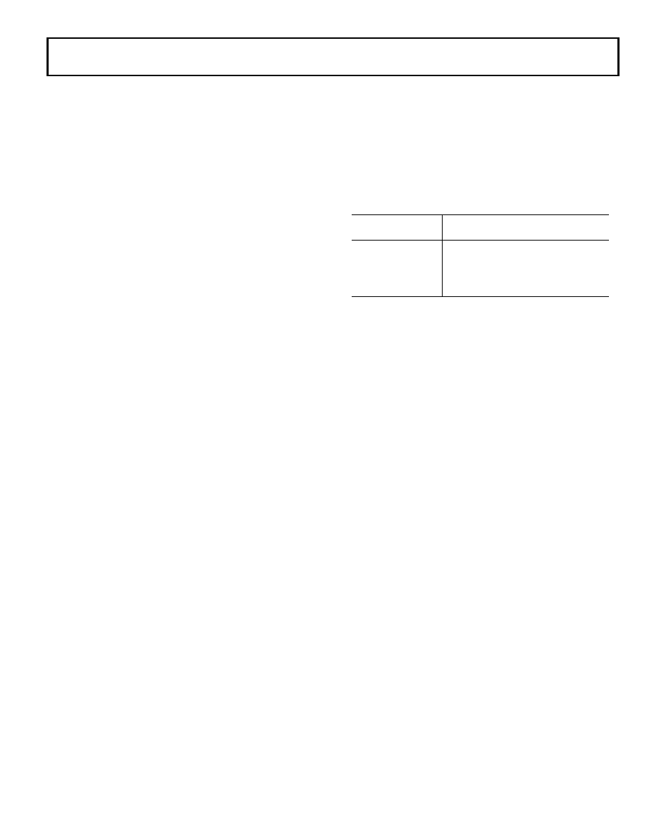
Table 17. Clock Periods
Timing
Requirements
Description
tCK
CLKIN Clock Period
tCCLK
Processor Core Clock Period
tPCLK
Peripheral Clock Period = 2 × tCCLK
tSDCLK
SDRAM Clock Period = (tCCLK) × SDCKR
相关PDF资料 |
PDF描述 |
|---|---|
| TAJC106M035SNJ | CAP TANT 10UF 35V 20% 2312 |
| GBM08DSEF-S243 | CONN EDGECARD 16POS .156 EYELET |
| M24308/4-5 | CONN D-SUB PLUG 50POS CRIMP |
| NTV1212MC | CONV DC/DC 1W 12VIN 12V DL 3KV |
| VI-B1Z-CY-F3 | CONVERTER MOD DC/DC 2V 20W |
相关代理商/技术参数 |
参数描述 |
|---|---|
| ADSP-21479SBC2-EP | 功能描述:IC DSP SHARC 266MHZ LP 制造商:analog devices inc. 系列:SHARC? 包装:托盘 零件状态:在售 类型:浮点 接口:DAI,DPI,EBI/EMI,I2C,SPI,SPORT,UART/USART 时钟速率:266MHz 非易失性存储器:ROM(4Mb) 片载 RAM:5Mb 电压 - I/O:3.30V 电压 - 内核:1.20V 工作温度:0°C ~ 70°C 安装类型:表面贴装 封装/外壳:196-LFBGA,CSPBGA 供应商器件封装:196-CSPBGA(12x12) 标准包装:1 |
| ADSP-21483KSWZ-2B | 制造商:AD 制造商全称:Analog Devices 功能描述:SHARC Processor |
| ADSP-21483KSWZ-3AB | 制造商:AD 制造商全称:Analog Devices 功能描述:SHARC Processor |
| ADSP-21483KSWZ-3B | 制造商:AD 制造商全称:Analog Devices 功能描述:SHARC Processor |
| ADSP-21483KSWZ-4B | 制造商:AD 制造商全称:Analog Devices 功能描述:SHARC Processor |
发布紧急采购,3分钟左右您将得到回复。