- 您现在的位置:买卖IC网 > PDF目录19507 > ADSP-21479KSWZ-2A (Analog Devices Inc)IC DSP SHARC 266MHZ LP 100LQFP PDF资料下载
参数资料
| 型号: | ADSP-21479KSWZ-2A |
| 厂商: | Analog Devices Inc |
| 文件页数: | 58/72页 |
| 文件大小: | 0K |
| 描述: | IC DSP SHARC 266MHZ LP 100LQFP |
| 标准包装: | 1 |
| 系列: | SHARC® |
| 类型: | 浮点 |
| 接口: | DAI,DPI,EBI/EMI,I²C,SPI,SPORT,UART/USART |
| 时钟速率: | 266MHz |
| 非易失内存: | ROM(4Mb) |
| 芯片上RAM: | 5Mb |
| 电压 - 输入/输出: | 3.30V |
| 电压 - 核心: | 1.20V |
| 工作温度: | 0°C ~ 70°C |
| 安装类型: | 表面贴装 |
| 封装/外壳: | 100-LQFP 裸露焊盘 |
| 供应商设备封装: | 100-LQFP-EP(14x14) |
| 包装: | 托盘 |
| 其它名称: | Q6418433 |
第1页第2页第3页第4页第5页第6页第7页第8页第9页第10页第11页第12页第13页第14页第15页第16页第17页第18页第19页第20页第21页第22页第23页第24页第25页第26页第27页第28页第29页第30页第31页第32页第33页第34页第35页第36页第37页第38页第39页第40页第41页第42页第43页第44页第45页第46页第47页第48页第49页第50页第51页第52页第53页第54页第55页第56页第57页当前第58页第59页第60页第61页第62页第63页第64页第65页第66页第67页第68页第69页第70页第71页第72页
Rev. A
|
Page 61 of 72
|
September 2011
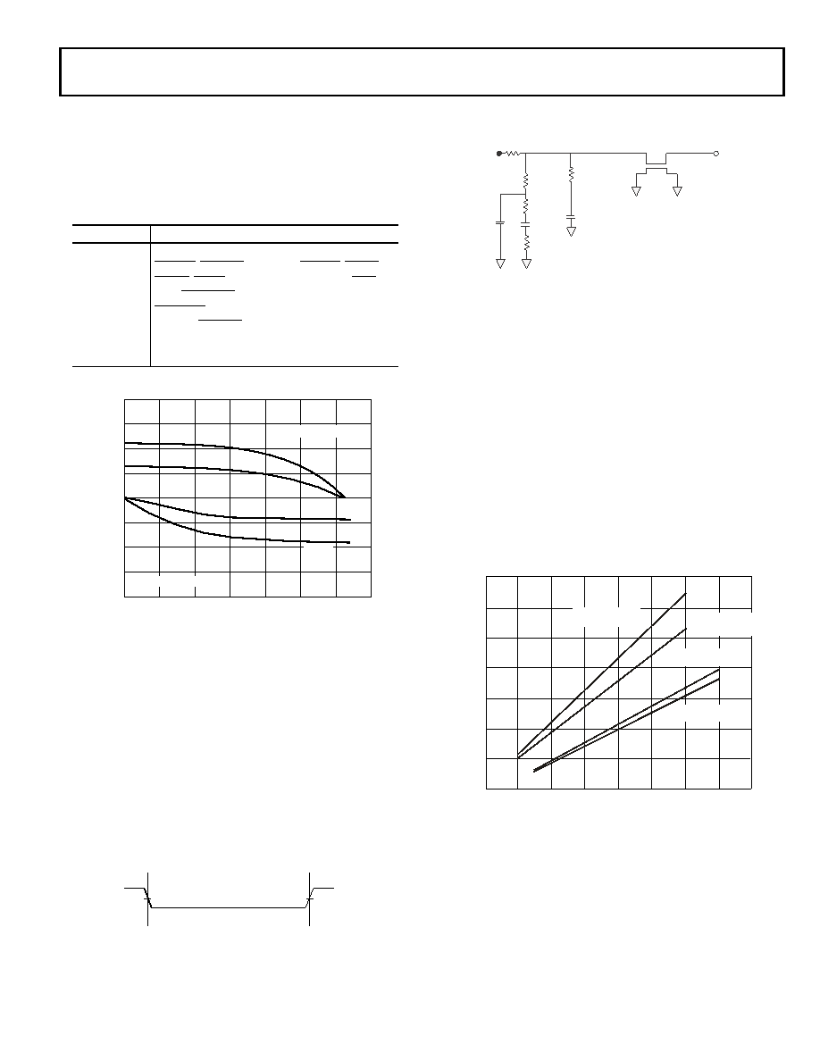
OUTPUT DRIVE CURRENTS
Table 55 shows the driver types and the pins associated with
each driver. Figure 47 shows typical I-V characteristics for each
driver. The curves represent the current drive capability of the
output drivers as a function of output voltage.
TEST CONDITIONS
The ac signal specifications (timing parameters) appear in
Table 20 on Page 26 through Table 54 on Page 60. These include
output disable time, output enable time, and capacitive loading.
The timing specifications for the SHARC apply for the voltage
reference levels in Figure 48.
Timing is measured on signals when they cross the 1.5 V level as
described in Figure 49. All delays (in nanoseconds) are mea-
sured between the point that the first signal reaches 1.5 V and
the point that the second signal reaches 1.5 V.
CAPACITIVE LOADING
Output delays and holds are based on standard capacitive loads:
how output delays and holds vary with load capacitance. The
outside the ranges shown for Typical Output Delay vs. Load
Capacitance and Typical Output Rise Time (20% to 80%,
V = Min) vs. Load Capacitance.
Table 55. Driver Types
Driver Type
Associated Pins
A
FLAG[0–3], AMI_ADDR[23–0], DATA[15–0],
AMI_RD, AMI_WR, AMI_ACK, MS[1-0], SDRAS,
SDCAS, SDWE, SDDQM, SDCKE, SDA10, EMU,
TDO, RESETOUT, DPI[1–14], DAI[1–20],
WDTRSTO, MLBDAT, MLBSIG, MLBSO, MLBDO,
MLBCLK, SR_CLR, SR_LAT, SR_LDO[17–0],
SR_SCLK, SR_SDI
BSDCLK, RTCLKOUT
Figure 47. Typical Drive at Junction Temperature
Figure 49. Voltage Reference Levels for AC Measurements
SWEEP (V
DDEXT) VOLTAGE (V)
0
3.5
0.5
1.0
1.5
2.0
2.5
3.0
0
100
200
SOURCE/SINK
(V
DDEXT
)CURRENT
(mA)
150
50
-100
-200
-150
-50
V
OH 3.13 V, 125 °C
V
OL 3.13 V, 125 °C
TYPE A
TYPE B
INPUT
OR
OUTPUT
1.5V
Figure 48. Equivalent Device Loading for AC Measurements
(Includes All Fixtures)
Figure 50. Typical Output Rise/Fall Time (20% to 80%,
VDD_EXT = Max)
T1
ZO = 50
: (impedance)
TD = 4.04
r 1.18 ns
2pF
TESTER PIN ELECTRONICS
50
:
0.5pF
70
:
400
:
45
:
4pF
NOTES:
THE WORST CASE TRANSMISSION LINE DELAY IS SHOWN AND CAN BE USED
FOR THE OUTPUT TIMING ANALYSIS TO REFLECT THE TRANSMISSION LINE
EFFECT AND MUST BE CONSIDERED. THE TRANSMISSION LINE (TD) IS FOR
LOAD ONLY AND DOES NOT AFFECT THE DATA SHEET TIMING SPECIFICATIONS.
ANALOG DEVICES RECOMMENDS USING THE IBIS MODEL TIMING FOR A GIVEN
SYSTEM REQUIREMENT. IF NECESSARY, A SYSTEM MAY INCORPORATE
EXTERNAL DRIVERS TO COMPENSATE FOR ANY TIMING DIFFERENCES.
VLOAD
DUT
OUTPUT
50
:
LOAD CAPACITANCE (pF)
6
0
7
4
2
1
3
RISE
AND
FALL
TIMES
(ns)
125
200
100
25
175
50
75
150
5
y = 0.0331x + 0.2662
y = 0.0184x + 0.3065
y = 0.0421x + 0.2418
y = 0.0206x + 0.2271
TYPE A DRIVE FALL
TYPE A DRIVE RISE
TYPE B DRIVE FALL
TYPE B DRIVE RISE
相关PDF资料 |
PDF描述 |
|---|---|
| TAJC106M035SNJ | CAP TANT 10UF 35V 20% 2312 |
| GBM08DSEF-S243 | CONN EDGECARD 16POS .156 EYELET |
| M24308/4-5 | CONN D-SUB PLUG 50POS CRIMP |
| NTV1212MC | CONV DC/DC 1W 12VIN 12V DL 3KV |
| VI-B1Z-CY-F3 | CONVERTER MOD DC/DC 2V 20W |
相关代理商/技术参数 |
参数描述 |
|---|---|
| ADSP-21479SBC2-EP | 功能描述:IC DSP SHARC 266MHZ LP 制造商:analog devices inc. 系列:SHARC? 包装:托盘 零件状态:在售 类型:浮点 接口:DAI,DPI,EBI/EMI,I2C,SPI,SPORT,UART/USART 时钟速率:266MHz 非易失性存储器:ROM(4Mb) 片载 RAM:5Mb 电压 - I/O:3.30V 电压 - 内核:1.20V 工作温度:0°C ~ 70°C 安装类型:表面贴装 封装/外壳:196-LFBGA,CSPBGA 供应商器件封装:196-CSPBGA(12x12) 标准包装:1 |
| ADSP-21483KSWZ-2B | 制造商:AD 制造商全称:Analog Devices 功能描述:SHARC Processor |
| ADSP-21483KSWZ-3AB | 制造商:AD 制造商全称:Analog Devices 功能描述:SHARC Processor |
| ADSP-21483KSWZ-3B | 制造商:AD 制造商全称:Analog Devices 功能描述:SHARC Processor |
| ADSP-21483KSWZ-4B | 制造商:AD 制造商全称:Analog Devices 功能描述:SHARC Processor |
发布紧急采购,3分钟左右您将得到回复。