- 您现在的位置:买卖IC网 > PDF目录19383 > ADSP-21991BBCZ (Analog Devices Inc)IC DSP CTLR 16BIT 196CSPBGA PDF资料下载
参数资料
| 型号: | ADSP-21991BBCZ |
| 厂商: | Analog Devices Inc |
| 文件页数: | 30/44页 |
| 文件大小: | 0K |
| 描述: | IC DSP CTLR 16BIT 196CSPBGA |
| 标准包装: | 1 |
| 系列: | ADSP-21xx |
| 类型: | 定点 |
| 接口: | SPI,SSP |
| 时钟速率: | 150MHz |
| 非易失内存: | 外部 |
| 芯片上RAM: | 112kB |
| 电压 - 输入/输出: | 3.30V |
| 电压 - 核心: | 2.50V |
| 工作温度: | -40°C ~ 85°C |
| 安装类型: | 表面贴装 |
| 封装/外壳: | 196-BGA |
| 供应商设备封装: | 196-MBGA(15x15) |
| 包装: | 托盘 |
第1页第2页第3页第4页第5页第6页第7页第8页第9页第10页第11页第12页第13页第14页第15页第16页第17页第18页第19页第20页第21页第22页第23页第24页第25页第26页第27页第28页第29页当前第30页第31页第32页第33页第34页第35页第36页第37页第38页第39页第40页第41页第42页第43页第44页
ADSP-21991
–36–
REV. 0
Output Enable Time
Output pins are considered to be enabled when they have made
a transition from a high impedance state to when they start
driving. The output enable time tENA is the interval from when a
reference signal reaches a high or low voltage level to when the
output has reached a specified high or low trip point, as shown
in the Output Enable/Disable diagram (Figure 18). If multiple
pins (such as the data bus) are enabled, the measurement value
is that of the first pin to start driving.
Example System Hold Time Calculation
To determine the data output hold time in a particular system,
on Page 35. Choose
V to be the difference between the output
voltage of the ADSP-21991 and the input threshold for the device
requiring the hold time. A typical
V will be 0.4 V. CLis the total
bus capacitance (per data line), and IL is the total leakage or three-
state current (per data line). The hold time will be tDECAY plus the
minimum disable time (i.e., tDATRWH for the write cycle).
Pin Configurations
Table 16 identifies the signal for each Mini-BGA ball number.
Table 17 identifies the Mini-BGA ball number for each signal
name.
Table 18 identifies the signal for each LQFP lead.
Table 19 identifies the LQFP lead for each signal name.
Table 4 describes each signal.
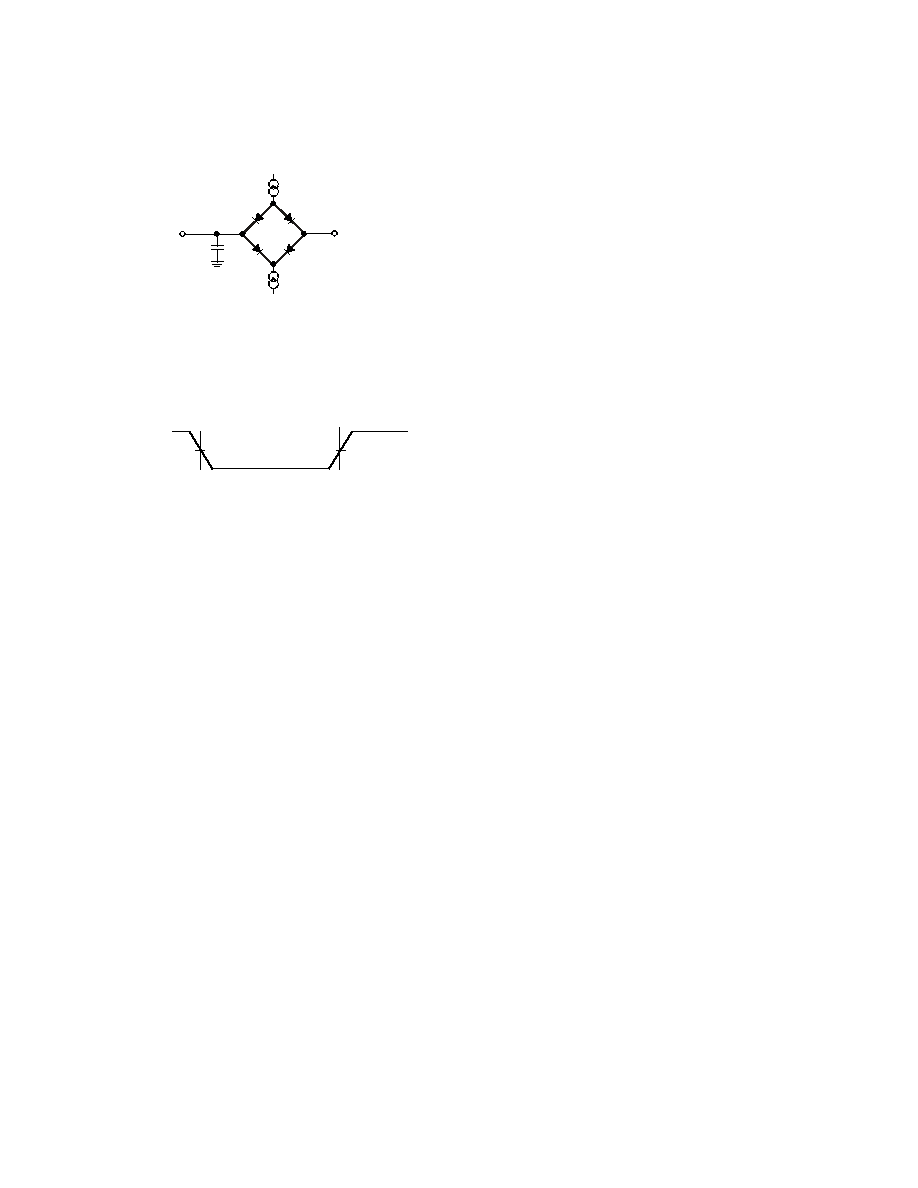
Figure 19. Equivalent Device Loading for AC
Measurements (Includes All Fixtures)
Figure 20. Voltage Reference Levels for AC
Measurements (Except Output Enable/Disable)
1.5V
50pF
TO
OUTPUT
PIN
IOL
IOH
INPUT
OR
OUTPUT
1.5V
相关PDF资料 |
PDF描述 |
|---|---|
| VI-B1V-CV-F3 | CONVERTER MOD DC/DC 5.8V 150W |
| RCM08DTAH-S189 | CONN EDGECARD 16POS R/A .156 SLD |
| VI-2NY-CX-F3 | CONVERTER MOD DC/DC 3.3V 49.5W |
| VI-2NY-CW-F1 | CONVERTER MOD DC/DC 3.3V 66W |
| 1130-332K-RC | CHOKE RF HI CURR 3300UH 10% RAD |
相关代理商/技术参数 |
参数描述 |
|---|---|
| ADSP-21991BST | 制造商:Analog Devices 功能描述:DSP Fixed-Point 16-Bit 160MHz 160MIPS 176-Pin LQFP 制造商:Rochester Electronics LLC 功能描述:HIGH PERFORMANCE MIXED SIGNAL DSP - Bulk |
| ADSP-21991BSTZ | 功能描述:IC DSP CONTROLLER 16BIT 176-LQFP RoHS:是 类别:集成电路 (IC) >> 嵌入式 - DSP(数字式信号处理器) 系列:ADSP-21xx 标准包装:2 系列:StarCore 类型:SC140 内核 接口:DSI,以太网,RS-232 时钟速率:400MHz 非易失内存:外部 芯片上RAM:1.436MB 电压 - 输入/输出:3.30V 电压 - 核心:1.20V 工作温度:-40°C ~ 105°C 安装类型:表面贴装 封装/外壳:431-BFBGA,FCBGA 供应商设备封装:431-FCPBGA(20x20) 包装:托盘 |
| ADSP-21992BBC | 制造商:Analog Devices 功能描述:DSP Fixed-Point 16-Bit 150MHz 150MIPS 196-Pin CSP-BGA 制造商:Rochester Electronics LLC 功能描述:MIXED SIGNAL DSP W/32K DM RAM& 16K PMRAM - Bulk |
| ADSP-21992BST | 制造商:Analog Devices 功能描述:DSP Fixed-Point 16-Bit 160MHz 160MIPS 176-Pin LQFP 制造商:Analog Devices 功能描述:IC MICROCOMPUTER 16-BIT |
| ADSP-21992BSTZ | 功能描述:IC DSP CONTROLLER 16BIT 176LQFP RoHS:是 类别:集成电路 (IC) >> 嵌入式 - DSP(数字式信号处理器) 系列:ADSP-21xx 标准包装:40 系列:TMS320DM64x, DaVinci™ 类型:定点 接口:I²C,McASP,McBSP 时钟速率:400MHz 非易失内存:外部 芯片上RAM:160kB 电压 - 输入/输出:3.30V 电压 - 核心:1.20V 工作温度:0°C ~ 90°C 安装类型:表面贴装 封装/外壳:548-BBGA,FCBGA 供应商设备封装:548-FCBGA(27x27) 包装:托盘 配用:TMDSDMK642-0E-ND - DEVELPER KIT W/NTSC CAMERA296-23038-ND - DSP STARTER KIT FOR TMS320C6416296-23059-ND - FLASHBURN PORTING KIT296-23058-ND - EVAL MODULE FOR DM642TMDSDMK642-ND - DEVELOPER KIT W/NTSC CAMERA |
发布紧急采购,3分钟左右您将得到回复。