- 您现在的位置:买卖IC网 > PDF目录15527 > ADSP-3PARCBF548E02 (Analog Devices Inc)KIT DEV STARTER BF548 PDF资料下载
参数资料
| 型号: | ADSP-3PARCBF548E02 |
| 厂商: | Analog Devices Inc |
| 文件页数: | 88/100页 |
| 文件大小: | 0K |
| 描述: | KIT DEV STARTER BF548 |
| 产品培训模块: | Arcturus uCBF54x-EMM |
| 特色产品: | uCBF54x Start Kit and System Module by Arcturus |
| 标准包装: | 1 |
| 系列: | Blackfin® |
| 类型: | DSP |
| 适用于相关产品: | ADSP-BF548 |
| 所含物品: | 板,线缆,CD,带麦克风的耳机,模块,电源 |
| 相关产品: | ADSP-BF548MBBCZ-5M-ND - IC DSP 533MHZ W/DDR 400CSPBGA ADSP-BF548BBCZ-5A-ND - IC DSP 16BIT 533MHZ 400CSBGA |
第1页第2页第3页第4页第5页第6页第7页第8页第9页第10页第11页第12页第13页第14页第15页第16页第17页第18页第19页第20页第21页第22页第23页第24页第25页第26页第27页第28页第29页第30页第31页第32页第33页第34页第35页第36页第37页第38页第39页第40页第41页第42页第43页第44页第45页第46页第47页第48页第49页第50页第51页第52页第53页第54页第55页第56页第57页第58页第59页第60页第61页第62页第63页第64页第65页第66页第67页第68页第69页第70页第71页第72页第73页第74页第75页第76页第77页第78页第79页第80页第81页第82页第83页第84页第85页第86页第87页当前第88页第89页第90页第91页第92页第93页第94页第95页第96页第97页第98页第99页第100页
Rev. C
|
Page 88 of 100
|
February 2010
ADSP-BF542/ADSP-BF544/ADSP-BF547/ADSP-BF548/ADSP-BF549
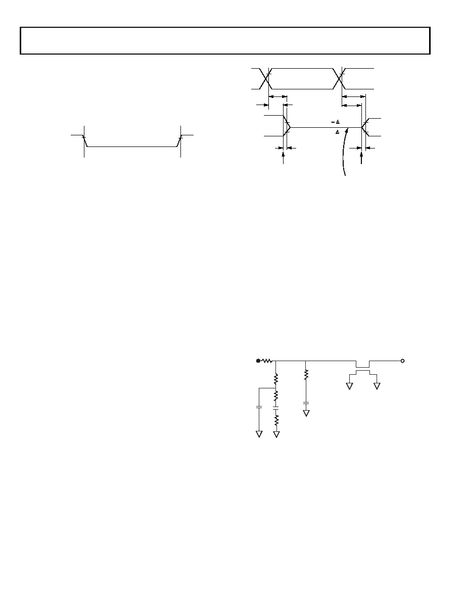
TEST CONDITIONS
All timing parameters appearing in this data sheet were mea-
sured under the conditions described in this section. Figure 71
shows the measurement point for AC measurements (except
output enable/disable). The measurement point VMEAS is
VDDEXT/2 or VDDDDR/2, depending on the pin under test.
Output Enable Time
Output pins are considered to be enabled when they have made
a transition from a high-impedance state to the point when they
start driving. The output enable time tENA is the interval from
the point when a reference signal reaches a high or low voltage
level to the point when the output starts driving as shown in the
output enable/disable diagram (Figure 72). The time,
tENA_MEASURED, is the interval from the point when the reference
signal switches to the point when the output voltage reaches
either 1.75 V (output high) or 1.25 V (output low). Time tTRIP is
the interval from when the output starts driving to when the
output reaches the 1.25 V or 1.75 V trip voltage. Time tENA is
calculated as shown in the equation:
If multiple pins (such as the data bus) are enabled, the measure-
ment value is that of the first pin to start driving.
Output Disable Time
Output pins are considered to be disabled when they stop driv-
ing, go into a high-impedance state, and start to decay from
their output high or low voltage. The time for the voltage on the
bus to decay by
V is dependent on the capacitive load, C
L and
the load current, IL. This decay time can be approximated by the
equation:
The output disable time tDIS is the difference between
tDIS_MEASURED is the interval from when the reference signal
switches to when the output voltage decays
V from the mea-
sured output high or output low voltage. The time tDECAY is
calculated with test loads CL and IL, and with V equal to 0.25 V.
Example System Hold Time Calculation
To determine the data output hold time in a particular system,
first calculate tDECAY using the equation given above. Choose V
to be the difference between the ADSP-BF54x Blackfin proces-
sors’ output voltage and the input threshold for the device
requiring the hold time. A typical
V will be 0.4 V. C
L is the total
bus capacitance (per data line), and IL is the total leakage or
three-state current (per data line). The hold time will be tDECAY
plus the minimum disable time (for example, tDDAT for an asyn-
chronous memory write cycle).
CAPACITIVE LOADING
Output delays and holds are based on standard capacitive loads
of an average of 6 pF on all balls (see Figure 73).
Figure 71. Voltage Reference Levels for AC Measurements
(Except Output Enable/Disable)
INPUT
OR
OUTPUT
VMEAS
t
ENA
t
ENA_MEASURED
t
TRIP
–
=
t
DECAY
C
L
V
() I
L
=
Figure 72. Output Enable/Disable
Figure 73. Equivalent Device Loading for AC Measurements
(Includes All Fixtures)
REFERENCE
SIGNAL
tDIS
OUTPUT STARTS DRIVING
VOH (MEASURED)
V
VOL (MEASURED) + V
tDIS_MEASURED
VOH
(MEASURED)
VOL
(MEASURED)
VTRIP(HIGH)
VOH(MEASURED)
VOL(MEASURED)
HIGH IMPEDANCE STATE
OUTPUT STOPS DRIVING
tENA
tDECAY
tENA_MEASURED
tTRIP
VTRIP(LOW)
T1
ZO = 50
(impedance)
TD = 4.04
1.18 ns
2pF
TESTER PIN ELECTRONICS
50
0.5pF
70
400
45
4pF
NOTES:
THE WORST-CASE TRANSMISSION LINE DELAY IS SHOWN AND CAN BE USED
FOR THE OUTPUT TIMING ANALYSIS TO REFELECT THE TRANSMISSION LINE
EFFECT AND MUST BE CONSIDERED. THE TRANSMISSION LINE (TD), IS FOR
LOAD ONLY AND DOES NOT AFFECT THE DATA SHEET TIMING SPECIFICATIONS.
ANALOG DEVICES RECOMMENDS USING THE IBIS MODEL TIMING FOR A GIVEN
SYSTEM REQUIREMENT. IF NECESSARY, A SYSTEM MAY INCORPORATE
EXTERNAL DRIVERS TO COMPENSATE FOR ANY TIMING DIFFERENCES.
VLOAD
DUT
OUTPUT
50
相关PDF资料 |
PDF描述 |
|---|---|
| ECM25DCTI-S288 | CONN EDGECARD 50POS .156 EXTEND |
| GCM18DTKI-S288 | CONN EDGECARD 36POS .156 EXTEND |
| UCC3957MTR-2 | IC LI-ION PROTECT CIRCUIT 16QSOP |
| GBM28DRMI-S288 | CONN EDGECARD 56POS .156 EXTEND |
| UCC3957MTR-1G4 | IC LI-ION PROTECT CIRCUIT 16QSOP |
相关代理商/技术参数 |
参数描述 |
|---|---|
| ADSP-3PARCBF548M01 | 功能描述:MODULE BOARD BF548 RoHS:是 类别:集成电路 (IC) >> 嵌入式 - 微控制器或微处理器模块 系列:Blackfin® 产品目录绘图:DLP-245SY-G 标准包装:1 系列:USB 模块/板类型:开发板 适用于相关产品:USB 其它名称:813-1006 |
| ADSP-BF504BCPZ-3F | 功能描述:IC CCD SIGNAL PROCESSOR 88LFCSP RoHS:是 类别:集成电路 (IC) >> 嵌入式 - DSP(数字式信号处理器) 系列:Blackfin® 标准包装:2 系列:StarCore 类型:SC140 内核 接口:DSI,以太网,RS-232 时钟速率:400MHz 非易失内存:外部 芯片上RAM:1.436MB 电压 - 输入/输出:3.30V 电压 - 核心:1.20V 工作温度:-40°C ~ 105°C 安装类型:表面贴装 封装/外壳:431-BFBGA,FCBGA 供应商设备封装:431-FCPBGA(20x20) 包装:托盘 |
| ADSP-BF504BCPZ-4 | 功能描述:IC CCD SIGNAL PROCESSOR 88LFCSP RoHS:是 类别:集成电路 (IC) >> 嵌入式 - DSP(数字式信号处理器) 系列:Blackfin® 标准包装:40 系列:TMS320DM64x, DaVinci™ 类型:定点 接口:I²C,McASP,McBSP 时钟速率:400MHz 非易失内存:外部 芯片上RAM:160kB 电压 - 输入/输出:3.30V 电压 - 核心:1.20V 工作温度:0°C ~ 90°C 安装类型:表面贴装 封装/外壳:548-BBGA,FCBGA 供应商设备封装:548-FCBGA(27x27) 包装:托盘 配用:TMDSDMK642-0E-ND - DEVELPER KIT W/NTSC CAMERA296-23038-ND - DSP STARTER KIT FOR TMS320C6416296-23059-ND - FLASHBURN PORTING KIT296-23058-ND - EVAL MODULE FOR DM642TMDSDMK642-ND - DEVELOPER KIT W/NTSC CAMERA |
| ADSP-BF504BCPZ-4F | 功能描述:IC CCD SIGNAL PROCESSOR 88LFCSP RoHS:是 类别:集成电路 (IC) >> 嵌入式 - DSP(数字式信号处理器) 系列:Blackfin® 标准包装:2 系列:StarCore 类型:SC140 内核 接口:DSI,以太网,RS-232 时钟速率:400MHz 非易失内存:外部 芯片上RAM:1.436MB 电压 - 输入/输出:3.30V 电压 - 核心:1.20V 工作温度:-40°C ~ 105°C 安装类型:表面贴装 封装/外壳:431-BFBGA,FCBGA 供应商设备封装:431-FCPBGA(20x20) 包装:托盘 |
| ADSP-BF504KCPZ-3F | 功能描述:IC CCD SIGNAL PROCESSOR 88LFCSP RoHS:是 类别:集成电路 (IC) >> 嵌入式 - DSP(数字式信号处理器) 系列:Blackfin® 标准包装:2 系列:StarCore 类型:SC140 内核 接口:DSI,以太网,RS-232 时钟速率:400MHz 非易失内存:外部 芯片上RAM:1.436MB 电压 - 输入/输出:3.30V 电压 - 核心:1.20V 工作温度:-40°C ~ 105°C 安装类型:表面贴装 封装/外壳:431-BFBGA,FCBGA 供应商设备封装:431-FCPBGA(20x20) 包装:托盘 |
发布紧急采购,3分钟左右您将得到回复。