- 您现在的位置:买卖IC网 > PDF目录19311 > ADSP-BF531SBB400 (Analog Devices Inc)IC DSP CTLR 16BIT 400MHZ 169-BGA PDF资料下载
参数资料
| 型号: | ADSP-BF531SBB400 |
| 厂商: | Analog Devices Inc |
| 文件页数: | 27/64页 |
| 文件大小: | 0K |
| 描述: | IC DSP CTLR 16BIT 400MHZ 169-BGA |
| 产品培训模块: | Blackfin® Processor Core Architecture Overview Blackfin® Device Drivers Blackfin® Optimizations for Performance and Power Consumption Blackfin® System Services |
| 产品变化通告: | Product Discontinuance 27/Oct/2011 |
| 标准包装: | 1 |
| 系列: | Blackfin® |
| 类型: | 定点 |
| 接口: | SPI,SSP,UART |
| 时钟速率: | 400MHz |
| 非易失内存: | ROM(1 kB) |
| 芯片上RAM: | 52kB |
| 电压 - 输入/输出: | 3.30V |
| 电压 - 核心: | 1.20V |
| 工作温度: | -40°C ~ 85°C |
| 安装类型: | 表面贴装 |
| 封装/外壳: | 169-BBGA |
| 供应商设备封装: | 169-PBGA(19x19) |
| 包装: | 托盘 |
| 配用: | ADZS-BF533-EZLITE-ND - KIT W/BOARD EVAL FOR ADSP-BF533 |
第1页第2页第3页第4页第5页第6页第7页第8页第9页第10页第11页第12页第13页第14页第15页第16页第17页第18页第19页第20页第21页第22页第23页第24页第25页第26页当前第27页第28页第29页第30页第31页第32页第33页第34页第35页第36页第37页第38页第39页第40页第41页第42页第43页第44页第45页第46页第47页第48页第49页第50页第51页第52页第53页第54页第55页第56页第57页第58页第59页第60页第61页第62页第63页第64页
�� �
�
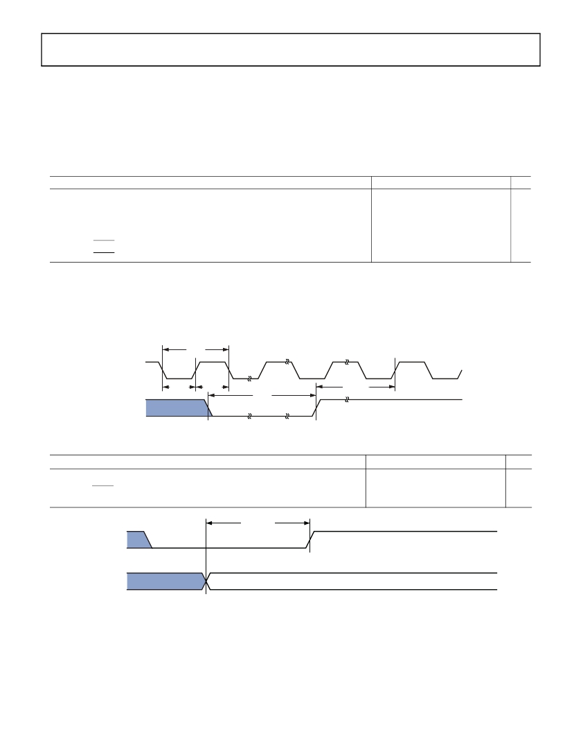
�ADSP-BF531� /� ADSP-BF532� /� ADSP-BF533�
�TIMING� SPECIFICATIONS�
�Clock� and� Reset� Timing�
���CLKIN� and� clock� multipliers/divisors� must� not� result� in� core/�
�Table� 21.� Clock� and� Reset� Timing�
�system� clocks� exceeding� the� maximum� limits� allowed� for� the�
�processor,� including� system� clock� restrictions� related� to� supply�
�voltage.�
�Parameter�
�Min�
�Max�
�Unit�
�Timing� Requirements�
�t� CKIN�
�t� CKINL�
�t� CKINH�
�t� WRST�
�t� NOBOOT�
�CLKIN� Period� 1,� 2,� 3,� 4�
�CLKIN� Low� Pulse�
�CLKIN� High� Pulse�
�RESET� Asserted� Pulse� Width� Low� 5�
�RESET� Deassertion� to� First� External� Access� Delay� 6�
�25.0�
�10.0�
�10.0�
�11� ?� t� CKIN�
�3� ?� t� CKIN�
�100.0�
�5� ?� t� CKIN�
�ns�
�ns�
�ns�
�ns�
�ns�
�1�
�2�
�3�
�4�
�5�
�6�
�Applies� to� PLL� bypass� mode� and� PLL� non� bypass� mode.�
�CLKIN� frequency� must� not� change� on� the� fly.�
�Combinations� of� the� CLKIN� frequency� and� the� PLL� clock� multiplier� must� not� exceed� the� allowed� f� VCO� ,� f� CCLK� ,� and� f� SCLK� settings� discussed� in� Table� 11� on� Page� 21� through�
�Table� 13� on� Page� 21� .� Since� the� default� behavior� of� the� PLL� is� to� multiply� the� CLKIN� frequency� by� 10,� the� 400� MHz� speed� grade� parts� cannot� use� the� full� CLKIN� period� range.�
�If� the� DF� bit� in� the� PLL_CTL� register� is� set,� then� the� maximum� t� CKIN� period� is� 50� ns.�
�Applies� after� power-up� sequence� is� complete.� See� Table� 22� and� Figure� 12� for� power-up� reset� timing.�
�Applies� when� processor� is� configured� in� No� Boot� Mode� (BMODE1-0� =� b#00).�
�t� CKIN�
�CLKIN�
�t� CKINL�
�t� CKINH�
�t� WRST�
�t� NOBOOT�
�RESET�
�Figure� 11.� Clock� and� Reset� Timing�
�Table� 22.� Power-Up� Reset� Timing�
�Parameter�
�Min�
�Max�
�Unit�
�Timing� Requirement�
�t� RST_IN_PWR�
�RESET� Deasserted� After� the� V� DDINT� ,� V� DDEXT� ,� V� DDRTC� ,� and� CLKIN� Pins� Are� Stable� and� 3500� ?� t� CKIN�
�Within� Specification�
�t� RST_IN_PWR�
�RESET�
�CLKIN�
�V�
�DD_SUPPLIES�
�In� Figure� 12� ,� V� DD_SUPPLIES� is� V� DDINT� ,� V� DDEXT� ,� V� DDRTC�
�Figure� 12.� Power-Up� Reset� Timing�
�ns�
�Rev.� I�
�|�
�Page� 27� of� 64� |�
�August� 2013�
�相关PDF资料 |
PDF描述 |
|---|---|
| ADSP-BF561SKB500 | IC DSP CTRLR 32BIT 500MHZ 297BGA |
| GEM10DTKN | CONN EDGECARD 20POS DIP .156 SLD |
| EEM11DRTH | CONN EDGECARD 22POS DIP .156 SLD |
| RSM36DRYI | CONN EDGECARD 72POS DIP .156 SLD |
| GEM10DTKH | CONN EDGECARD 20POS DIP .156 SLD |
相关代理商/技术参数 |
参数描述 |
|---|---|
| ADSPBF531SBBC400 | 制造商:Analog Devices 功能描述: |
| ADSP-BF531SBBC400 | 功能描述:IC DSP CTLR 16B 400MHZ 160MBGA RoHS:否 类别:集成电路 (IC) >> 嵌入式 - DSP(数字式信号处理器) 系列:Blackfin® 标准包装:2 系列:StarCore 类型:SC140 内核 接口:DSI,以太网,RS-232 时钟速率:400MHz 非易失内存:外部 芯片上RAM:1.436MB 电压 - 输入/输出:3.30V 电压 - 核心:1.20V 工作温度:-40°C ~ 105°C 安装类型:表面贴装 封装/外壳:431-BFBGA,FCBGA 供应商设备封装:431-FCPBGA(20x20) 包装:托盘 |
| ADSP-BF531SBBC-400X | 制造商:Analog Devices 功能描述: |
| ADSP-BF531SBBC-ENG | 制造商:Analog Devices 功能描述: |
| ADSP-BF531SBBCZ400 | 功能描述:IC DSP CTLR 16 400MHZ 160CSPBGA RoHS:是 类别:集成电路 (IC) >> 嵌入式 - DSP(数字式信号处理器) 系列:Blackfin® 标准包装:40 系列:TMS320DM64x, DaVinci™ 类型:定点 接口:I²C,McASP,McBSP 时钟速率:400MHz 非易失内存:外部 芯片上RAM:160kB 电压 - 输入/输出:3.30V 电压 - 核心:1.20V 工作温度:0°C ~ 90°C 安装类型:表面贴装 封装/外壳:548-BBGA,FCBGA 供应商设备封装:548-FCBGA(27x27) 包装:托盘 配用:TMDSDMK642-0E-ND - DEVELPER KIT W/NTSC CAMERA296-23038-ND - DSP STARTER KIT FOR TMS320C6416296-23059-ND - FLASHBURN PORTING KIT296-23058-ND - EVAL MODULE FOR DM642TMDSDMK642-ND - DEVELOPER KIT W/NTSC CAMERA |
发布紧急采购,3分钟左右您将得到回复。