- 您现在的位置:买卖IC网 > PDF目录19388 > ADSP-BF533SBBC-5V (Analog Devices Inc)IC DSP CTLR DUAL 160CSPBGA PDF资料下载
参数资料
| 型号: | ADSP-BF533SBBC-5V |
| 厂商: | Analog Devices Inc |
| 文件页数: | 41/64页 |
| 文件大小: | 0K |
| 描述: | IC DSP CTLR DUAL 160CSPBGA |
| 产品培训模块: | Blackfin® Processor Core Architecture Overview Blackfin® Device Drivers Blackfin® Optimizations for Performance and Power Consumption Blackfin® System Services |
| 标准包装: | 1 |
| 系列: | Blackfin® |
| 类型: | 定点 |
| 接口: | SPI,SSP,UART |
| 时钟速率: | 533MHz |
| 非易失内存: | ROM(1 kB) |
| 芯片上RAM: | 148kB |
| 电压 - 输入/输出: | 3.30V |
| 电压 - 核心: | 1.20V |
| 工作温度: | -40°C ~ 85°C |
| 安装类型: | 表面贴装 |
| 封装/外壳: | 160-LFBGA,CSPBGA |
| 供应商设备封装: | 160-CSPBGA(12x12) |
| 包装: | 托盘 |
| 配用: | ADZS-BFAUDIO-EZEXT-ND - BOARD EVAL AUDIO BLACKFIN ADZS-BFAV-EZEXT-ND - BOARD DAUGHT ADSP-BF533,37,61KIT ADZS-BF533-EZLITE-ND - KIT W/BOARD EVAL FOR ADSP-BF533 |
第1页第2页第3页第4页第5页第6页第7页第8页第9页第10页第11页第12页第13页第14页第15页第16页第17页第18页第19页第20页第21页第22页第23页第24页第25页第26页第27页第28页第29页第30页第31页第32页第33页第34页第35页第36页第37页第38页第39页第40页当前第41页第42页第43页第44页第45页第46页第47页第48页第49页第50页第51页第52页第53页第54页第55页第56页第57页第58页第59页第60页第61页第62页第63页第64页
�� �
�
�ADSP-BF531� /� ADSP-BF532� /� ADSP-BF533�
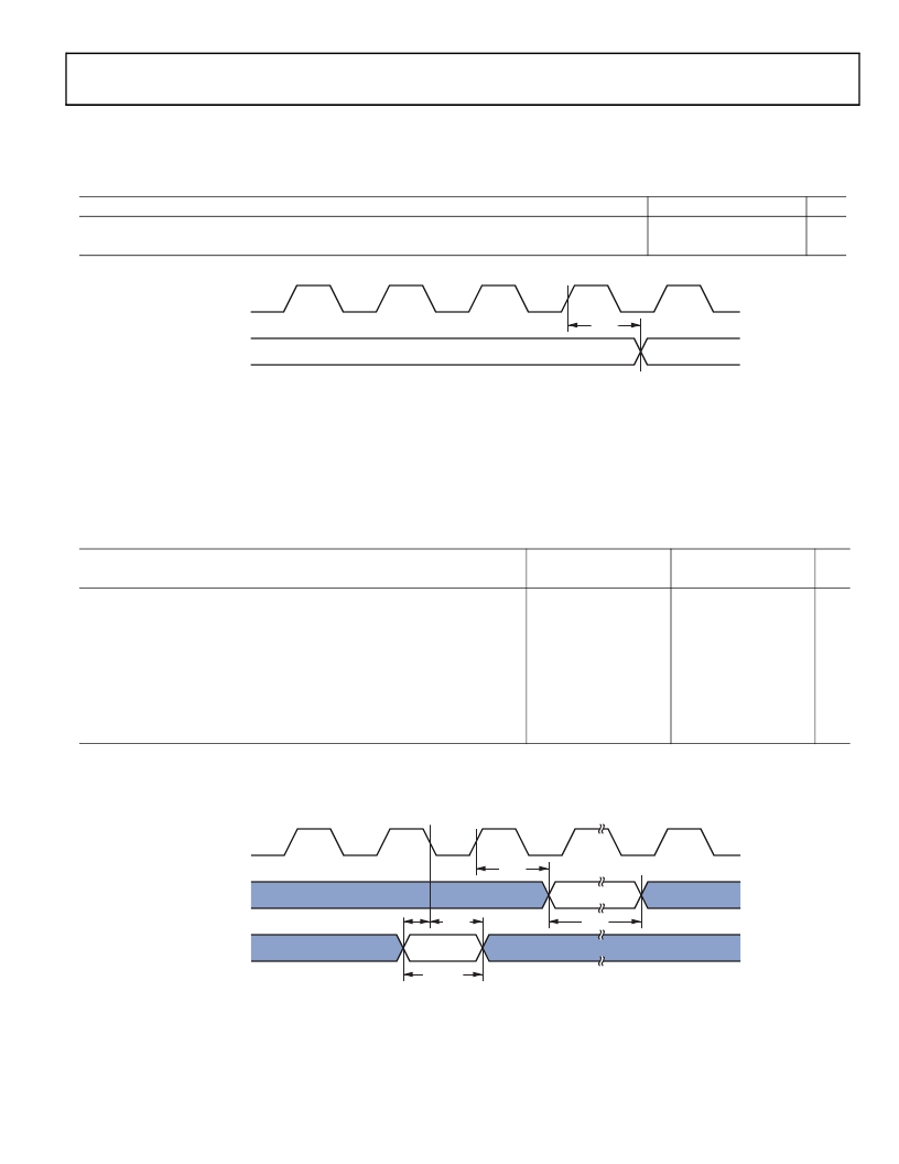
�Timer� Clock� Timing�
��Table� 35.� Timer� Clock� Timing�
�Parameter�
�Min�
�Max�
�Unit�
�Switching� Characteristic�
�t� TODP�
�Timer� Output� Update� Delay� After� PPI_CLK� High�
�12�
�ns�
�PPI_CLK�
�t� TODP�
�TMRx� OUTPUT�
�Figure� 30.� Timer� Clock� Timing�
�Timer� Cycle� Timing�
��input� signal� is� asynchronous� in� width� capture� mode� and� exter-�
�nal� clock� mode� and� has� an� absolute� maximum� input� frequency�
�of� f� SCLK� /2� MHz.�
�Table� 36.� Timer� Cycle� Timing�
�V� DDEXT� =� 1.8� V�
�V� DDEXT� =� 2.5� V/3.3� V�
�Parameter�
�Min� Max�
�Min� Max�
�Unit�
�Timing� Characteristics�
�t� WL� Timer� Pulse� Width� Low� 1�
�t� WH� Timer� Pulse� Width� High� 1�
�t� TIS� Timer� Input� Setup� Time� Before� CLKOUT� Low� 2�
�t� TIH� Timer� Input� Hold� Time� After� CLKOUT� Low� 2�
�1� � t� SCLK�
�1� � t� SCLK�
�8.0�
�1.5�
�1� � t� SCLK�
�1� � t� SCLK�
�6.5�
�1.5�
�ns�
�ns�
�ns�
�ns�
�Switching� Characteristic� s�
�t� HTO� Timer� Pulse� Width� Output�
�t� TOD� Timer� Output� Update� Delay� After� CLKOUT� High�
�1� � t� SCLK�
�(2� 32� –1)� ×� t� SCLK�
�7.5�
�1� � t� SCLK�
�(2� 32� –1)� ×� t� SCLK�
�6.5�
�ns�
�ns�
�1�
�2�
�The� minimum� pulse� widths� apply� for� TMRx� input� pins� in� width� capture� and� external� clock� modes.� They� also� apply� to� the� PF1� or� PPI_CLK� input� pins� in� PWM� output� mode.�
�Either� a� valid� setup� and� hold� time� or� a� valid� pulse� width� is� sufficient.� There� is� no� need� to� resynchronize� programmable� flag� inputs.�
�CLKOUT�
�t� TOD�
�TMRx� OUTPUT�
�t� TIS�
�t� TIH�
�t� HTO�
�TMRx� INPUT�
�t� WH� ,t� WL�
�Figure� 31.� Timer� PWM_OUT� Cycle� Timing�
�Rev.� I�
�|�
�Page� 41� of� 64� |�
�August� 2013�
�相关PDF资料 |
PDF描述 |
|---|---|
| SWS60015 | PWR SUP 15V 40A SNG OUTPUT |
| ADSP-BF537BBCZ-5B | IC DSP CTLR 16BIT 208CSPBGA |
| ADSP-BF534YBCZ-4B | IC DSP CTLR 16BIT 400MHZ 208-CSP |
| ADSP-21488BSWZ-3A | IC DSP 3MBIT 400MHZ 100LQFP |
| ADSP-BF544MBBCZ-5M | IC DSP 16BIT 533MHZ MDDR 400CBGA |
相关代理商/技术参数 |
参数描述 |
|---|---|
| ADSP-BF533SBBC-C10 | 制造商:Analog Devices 功能描述: |
| ADSP-BF533SBBC-C53 | 制造商:Analog Devices 功能描述: |
| ADSP-BF533SBBC-C73 | 制造商:Analog Devices 功能描述: |
| ADSP-BF533SBBC-ENG | 制造商:Analog Devices 功能描述: |
| ADSP-BF533SBBCZ | 制造商:Analog Devices 功能描述:- Trays |
发布紧急采购,3分钟左右您将得到回复。