- 您现在的位置:买卖IC网 > PDF目录19388 > ADSP-BF533SBBC-5V (Analog Devices Inc)IC DSP CTLR DUAL 160CSPBGA PDF资料下载
参数资料
| 型号: | ADSP-BF533SBBC-5V |
| 厂商: | Analog Devices Inc |
| 文件页数: | 5/64页 |
| 文件大小: | 0K |
| 描述: | IC DSP CTLR DUAL 160CSPBGA |
| 产品培训模块: | Blackfin® Processor Core Architecture Overview Blackfin® Device Drivers Blackfin® Optimizations for Performance and Power Consumption Blackfin® System Services |
| 标准包装: | 1 |
| 系列: | Blackfin® |
| 类型: | 定点 |
| 接口: | SPI,SSP,UART |
| 时钟速率: | 533MHz |
| 非易失内存: | ROM(1 kB) |
| 芯片上RAM: | 148kB |
| 电压 - 输入/输出: | 3.30V |
| 电压 - 核心: | 1.20V |
| 工作温度: | -40°C ~ 85°C |
| 安装类型: | 表面贴装 |
| 封装/外壳: | 160-LFBGA,CSPBGA |
| 供应商设备封装: | 160-CSPBGA(12x12) |
| 包装: | 托盘 |
| 配用: | ADZS-BFAUDIO-EZEXT-ND - BOARD EVAL AUDIO BLACKFIN ADZS-BFAV-EZEXT-ND - BOARD DAUGHT ADSP-BF533,37,61KIT ADZS-BF533-EZLITE-ND - KIT W/BOARD EVAL FOR ADSP-BF533 |
第1页第2页第3页第4页当前第5页第6页第7页第8页第9页第10页第11页第12页第13页第14页第15页第16页第17页第18页第19页第20页第21页第22页第23页第24页第25页第26页第27页第28页第29页第30页第31页第32页第33页第34页第35页第36页第37页第38页第39页第40页第41页第42页第43页第44页第45页第46页第47页第48页第49页第50页第51页第52页第53页第54页第55页第56页第57页第58页第59页第60页第61页第62页第63页第64页
�� �
�
�ADSP-BF531� /� ADSP-BF532� /� ADSP-BF533�
�ADDRESS� ARITHMETIC� UNIT�
�SP�
�I3�
�I2�
�L3�
�L2�
�B3�
�B2�
�M3�
�M2�
�FP�
�P5�
�I1�
�L1�
�B1�
�M1�
�DAG1�
�P4�
�DA1� 32�
�DA0� 32�
�I0�
�L0�
�B0�
�M0�
�DAG0�
�P3�
�P2�
�P1�
�P0�
�32�
�RAB�
�32�
�PREG�
�SD� 32�
�LD1� 32�
�LD0� 32�
�R7.H�
�R6.H�
�32�
�R7.L�
�R6.L�
�32�
�ASTAT�
�SEQUENCER�
�R5.H�
�R4.H�
�R3.H�
�R2.H�
�R5.L�
�R4.L�
�R3.L�
�R2.L�
�8�
�16�
�8�
�8�
�16�
�8�
�ALIGN�
�DECODE�
�R1.H�
�R0.H�
�R1.L�
�R0.L�
�BARREL�
�SHIFTER�
�A0�
�40�
�40�
�40�
�40�
�A1�
�LOOP� BUFFER�
�CONTROL�
�UNIT�
�32�
�32�
�DATA� ARITHMETIC� UNIT�
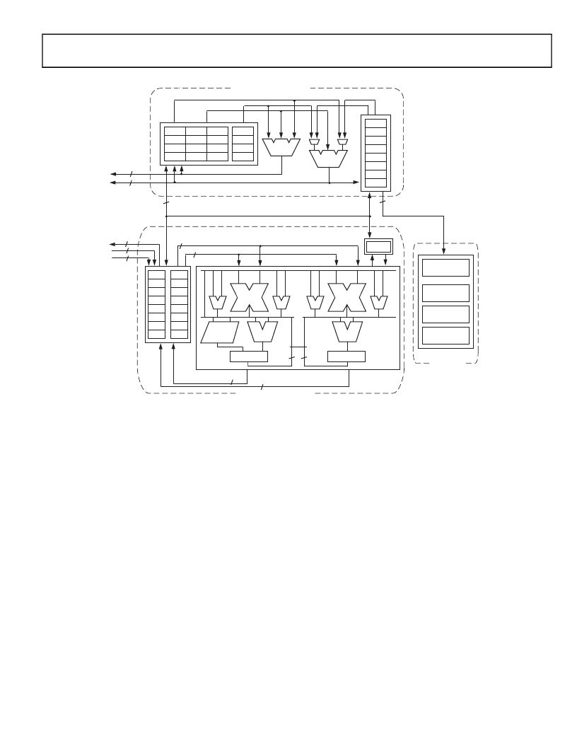
�Figure� 2.� Blackfin� Processor� Core�
�The� second� on-chip� memory� block� is� the� L1� data� memory,� con-�
�sisting� of� one� or� two� banks� of� up� to� 32K� bytes.� The� memory�
�banks� are� configurable,� offering� both� cache� and� SRAM� func-�
�tionality.� This� memory� block� is� accessed� at� full� processor� speed.�
�The� third� memory� block� is� a� 4K� byte� scratchpad� SRAM,� which�
�runs� at� the� same� speed� as� the� L1� memories,� but� is� only� accessible�
�as� data� SRAM� and� cannot� be� configured� as� cache� memory.�
�External� (Off-Chip)� Memory�
�External� memory� is� accessed� via� the� external� bus� interface� unit�
�(EBIU).� This� 16-bit� interface� provides� a� glueless� connection� to� a�
�bank� of� synchronous� DRAM� (SDRAM)� as� well� as� up� to� four�
�banks� of� asynchronous� memory� devices� including� flash,�
�EPROM,� ROM,� SRAM,� and� memory� mapped� I/O� devices.�
�The� PC133-compliant� SDRAM� controller� can� be� programmed�
�to� interface� to� up� to� 128M� bytes� of� SDRAM.� The� SDRAM� con-�
�troller� allows� one� row� to� be� open� for� each� internal� SDRAM�
�bank,� for� up� to� four� internal� SDRAM� banks,� improving� overall�
�system� performance.�
�The� asynchronous� memory� controller� can� be� programmed� to�
�control� up� to� four� banks� of� devices� with� very� flexible� timing�
�parameters� for� a� wide� variety� of� devices.� Each� bank� occupies� a�
�1M� byte� segment� regardless� of� the� size� of� the� devices� used,� so�
�that� these� banks� are� only� contiguous� if� each� is� fully� populated�
�with� 1M� byte� of� memory.�
�I/O� Memory� Space�
�Blackfin� processors� do� not� define� a� separate� I/O� space.� All�
�resources� are� mapped� through� the� flat� 32-bit� address� space.�
�On-chip� I/O� devices� have� their� control� registers� mapped� into�
�memory� mapped� registers� (MMRs)� at� addresses� near� the� top� of�
�the� 4G� byte� address� space.� These� are� separated� into� two� smaller�
�blocks,� one� containing� the� control� MMRs� for� all� core� functions,�
�and� the� other� containing� the� registers� needed� for� setup� and� con-�
�trol� of� the� on-chip� peripherals� outside� of� the� core.� The� MMRs�
�are� accessible� only� in� supervisor� mode� and� appear� as� reserved�
�space� to� on-chip� peripherals.�
�Booting�
�The� ADSP-BF531/ADSP-BF532/ADSP-BF533� processors� con-�
�tain� a� small� boot� kernel,� which� configures� the� appropriate�
�peripheral� for� booting.� If� the� processors� are� configured� to� boot�
�from� boot� ROM� memory� space,� the� processor� starts� executing�
�from� the� on-chip� boot� ROM.� For� more� information,� see� Boot-�
��Rev.� I�
�|�
�Page� 5� of� 64� |�
�August� 2013�
�相关PDF资料 |
PDF描述 |
|---|---|
| SWS60015 | PWR SUP 15V 40A SNG OUTPUT |
| ADSP-BF537BBCZ-5B | IC DSP CTLR 16BIT 208CSPBGA |
| ADSP-BF534YBCZ-4B | IC DSP CTLR 16BIT 400MHZ 208-CSP |
| ADSP-21488BSWZ-3A | IC DSP 3MBIT 400MHZ 100LQFP |
| ADSP-BF544MBBCZ-5M | IC DSP 16BIT 533MHZ MDDR 400CBGA |
相关代理商/技术参数 |
参数描述 |
|---|---|
| ADSP-BF533SBBC-C10 | 制造商:Analog Devices 功能描述: |
| ADSP-BF533SBBC-C53 | 制造商:Analog Devices 功能描述: |
| ADSP-BF533SBBC-C73 | 制造商:Analog Devices 功能描述: |
| ADSP-BF533SBBC-ENG | 制造商:Analog Devices 功能描述: |
| ADSP-BF533SBBCZ | 制造商:Analog Devices 功能描述:- Trays |
发布紧急采购,3分钟左右您将得到回复。