- 您现在的位置:买卖IC网 > PDF目录19370 > ADSP-TS201SABP-050 (Analog Devices Inc)IC PROCESSOR 500MHZ 576BGA PDF资料下载
参数资料
| 型号: | ADSP-TS201SABP-050 |
| 厂商: | Analog Devices Inc |
| 文件页数: | 15/48页 |
| 文件大小: | 0K |
| 描述: | IC PROCESSOR 500MHZ 576BGA |
| 标准包装: | 1 |
| 系列: | TigerSHARC® |
| 类型: | 定点/浮点 |
| 接口: | 主机接口,连接端口,多处理器 |
| 时钟速率: | 500MHz |
| 非易失内存: | 外部 |
| 芯片上RAM: | 3MB |
| 电压 - 输入/输出: | 2.50V |
| 电压 - 核心: | 1.05V |
| 工作温度: | -40°C ~ 85°C |
| 安装类型: | 表面贴装 |
| 封装/外壳: | 576-BBGA 裸露焊盘 |
| 供应商设备封装: | 576-BGA-ED(25x25) |
| 包装: | 托盘 |
| 配用: | ADZS-TS201S-EZLITE-ND - KIT LITE EVAL FOR ADSP-TS201S |
第1页第2页第3页第4页第5页第6页第7页第8页第9页第10页第11页第12页第13页第14页当前第15页第16页第17页第18页第19页第20页第21页第22页第23页第24页第25页第26页第27页第28页第29页第30页第31页第32页第33页第34页第35页第36页第37页第38页第39页第40页第41页第42页第43页第44页第45页第46页第47页第48页
Rev. C
|
Page 22 of 48
|
December 2006
ADSP-TS201S
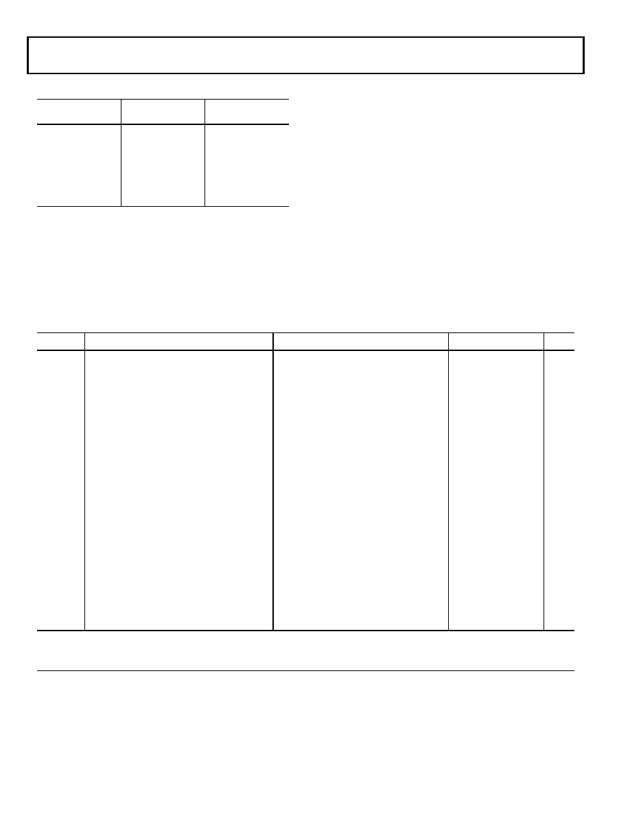
ELECTRICAL CHARACTERISTICS
Table 18. Maximum Duty Cycle for Input Transient Voltage
VIN Max (V)
1
VIN Min (V)
1
Maximum Duty
Cycle2
+3.63
–0.33
100%
+3.64
–0.34
90%
+3.70
–0.40
50%
+3.78
–0.48
30%
+3.86
–0.56
17%
+3.93
–0.63
10%
1 The individual values cannot be combined for analysis of a single instance of
overshoot or undershoot. The worst case observed value must fall within one of
the voltages specified and the total duration of the overshoot or undershoot
(exceeding the 100% case) must be less than or equal to the corresponding duty
cycle.
2 Duty cycle refers to the percentage of time the signal exceeds the value for the
100% case. This is equivalent to the measured duration of a single instance of
overshoot or undershoot as a percentage of the period of occurrence. The
practical worst case for period of occurrence for either overshoot or undershoot
is 2 × tSCLK.
Parameter Description
Test Conditions
Min
Max
Unit
VOH
High Level Output Voltage
1
1 Applies to output and bidirectional pins.
@VDD_IO =Min, IOH = –2 mA
2.18
V
VOL
Low Level Output Voltage
@VDD_IO =Min, IOL =4 mA
0.4
V
IIH
High Level Input Current
@VDD_IO =Max, VIN =VIH Max
20
μA
IIH_PU
High Level Input Current
@VDD_IO =Max, VIN =VIH Max
20
μA
IIH_PD
High Level Input Current
@VDD_IO =Max, VIN =VDD_IO Max
0.3
0.76
mA
IIH_PD_L
High Level Input Current
@VDD_IO =Max, VIN =VIH Max
3076μA
IIL
Low Level Input Current
@VDD_IO =Max, VIN =0 V
20
μA
IIL_PU
Low Level Input Current
@VDD_IO =Max, VIN =0 V
0.3
0.76
mA
IIL_PU_AD
Low Level Input Current
@VDD_IO =Max, VIN = 0 V
30
100
μA
IOZH
Three-State Leakage Current High
@VDD_IO =Max, VIN =VIH Max
50
μA
IOZH_PD
Three-State Leakage Current High
@VDD_IO =Max, VIN =VDD_IO Max
0.3
0.76
mA
IOZL
Three-State Leakage Current Low
@VDD_IO =Max, VIN =0 V
20
μA
IOZL_PU
Three-State Leakage Current Low
@VDD_IO =Max, VIN =0 V
0.3
0.76
mA
IOZL_PU_AD
Three-State Leakage Current Low
@VDD_IO =Max, VIN = 0 V
30
100
μA
IOZL_OD
Three-State Leakage Current Low
@VDD_IO =Max, VIN =0 V
4
7.6
mA
CIN
Input Capacitance
2, 3
2 Applies to all signals.
3 Guaranteed but not tested.
@fIN =1 MHz, TCASE =25°C, VIN =2.5 V
3
pF
Parameter name suffix conventions: no suffix = applies to pins without pull-up or pull-down resistors, _PD = applies to pin types (pd) or
(pd_0), _PU = applies to pin types (pu) or (pu_0), _PU_AD = applies to pin types (pu_ad), _OD = applies to pin types OD, _PD_L = applies
to pin types (pd_l)
相关PDF资料 |
PDF描述 |
|---|---|
| ADSP-TS101SAB2-100 | IC DSP CONTROLLER 6MBIT 484 BGA |
| VE-B34-CY-S | CONVERTER MOD DC/DC 48V 50W |
| ATFC-0402-1N0-BT | INDUCTOR THIN FILM 1.0NH 0402 |
| ADSP-TS201SABPZ050 | IC PROCESSOR 500MHZ 576BGA |
| TAJY475M050RNJ | CAP TANT 4.7UF 50V 20% 2917 |
相关代理商/技术参数 |
参数描述 |
|---|---|
| ADSP-TS201SABP-060 | 功能描述:IC PROCESSOR 600MHZ 576BGA RoHS:否 类别:集成电路 (IC) >> 嵌入式 - DSP(数字式信号处理器) 系列:TigerSHARC® 标准包装:2 系列:StarCore 类型:SC140 内核 接口:DSI,以太网,RS-232 时钟速率:400MHz 非易失内存:外部 芯片上RAM:1.436MB 电压 - 输入/输出:3.30V 电压 - 核心:1.20V 工作温度:-40°C ~ 105°C 安装类型:表面贴装 封装/外壳:431-BFBGA,FCBGA 供应商设备封装:431-FCPBGA(20x20) 包装:托盘 |
| ADSP-TS201SABP-10X | 制造商:Analog Devices 功能描述: |
| ADSP-TS201SABP-15X | 制造商:Analog Devices 功能描述: |
| ADSP-TS201SABP-ENG | 制造商:Analog Devices 功能描述: |
| ADSP-TS201SABP-ENG1 | 制造商:Analog Devices 功能描述: |
发布紧急采购,3分钟左右您将得到回复。