- 您现在的位置:买卖IC网 > PDF目录19370 > ADSP-TS201SABP-050 (Analog Devices Inc)IC PROCESSOR 500MHZ 576BGA PDF资料下载
参数资料
| 型号: | ADSP-TS201SABP-050 |
| 厂商: | Analog Devices Inc |
| 文件页数: | 32/48页 |
| 文件大小: | 0K |
| 描述: | IC PROCESSOR 500MHZ 576BGA |
| 标准包装: | 1 |
| 系列: | TigerSHARC® |
| 类型: | 定点/浮点 |
| 接口: | 主机接口,连接端口,多处理器 |
| 时钟速率: | 500MHz |
| 非易失内存: | 外部 |
| 芯片上RAM: | 3MB |
| 电压 - 输入/输出: | 2.50V |
| 电压 - 核心: | 1.05V |
| 工作温度: | -40°C ~ 85°C |
| 安装类型: | 表面贴装 |
| 封装/外壳: | 576-BBGA 裸露焊盘 |
| 供应商设备封装: | 576-BGA-ED(25x25) |
| 包装: | 托盘 |
| 配用: | ADZS-TS201S-EZLITE-ND - KIT LITE EVAL FOR ADSP-TS201S |
第1页第2页第3页第4页第5页第6页第7页第8页第9页第10页第11页第12页第13页第14页第15页第16页第17页第18页第19页第20页第21页第22页第23页第24页第25页第26页第27页第28页第29页第30页第31页当前第32页第33页第34页第35页第36页第37页第38页第39页第40页第41页第42页第43页第44页第45页第46页第47页第48页
Rev. C
|
Page 38 of 48
|
December 2006
ADSP-TS201S
Output Enable Time
Output pins are considered to be enabled when they have made
a transition from a high impedance state to when they start driv-
ing. The time for the voltage on the bus to ramp by
ΔV is
dependent on the capacitive load, CL, and the drive current, ID.
This ramp time can be approximated by the following equation:
The output enable time tENA is the difference between
tMEASURED_ENA is the interval from when the reference signal
switches to when the output voltage ramps
ΔV from the mea-
sured three-stated output level. tRAMP is calculated with test load
CL, drive current ID, and with
ΔV equal to 0.4 V.
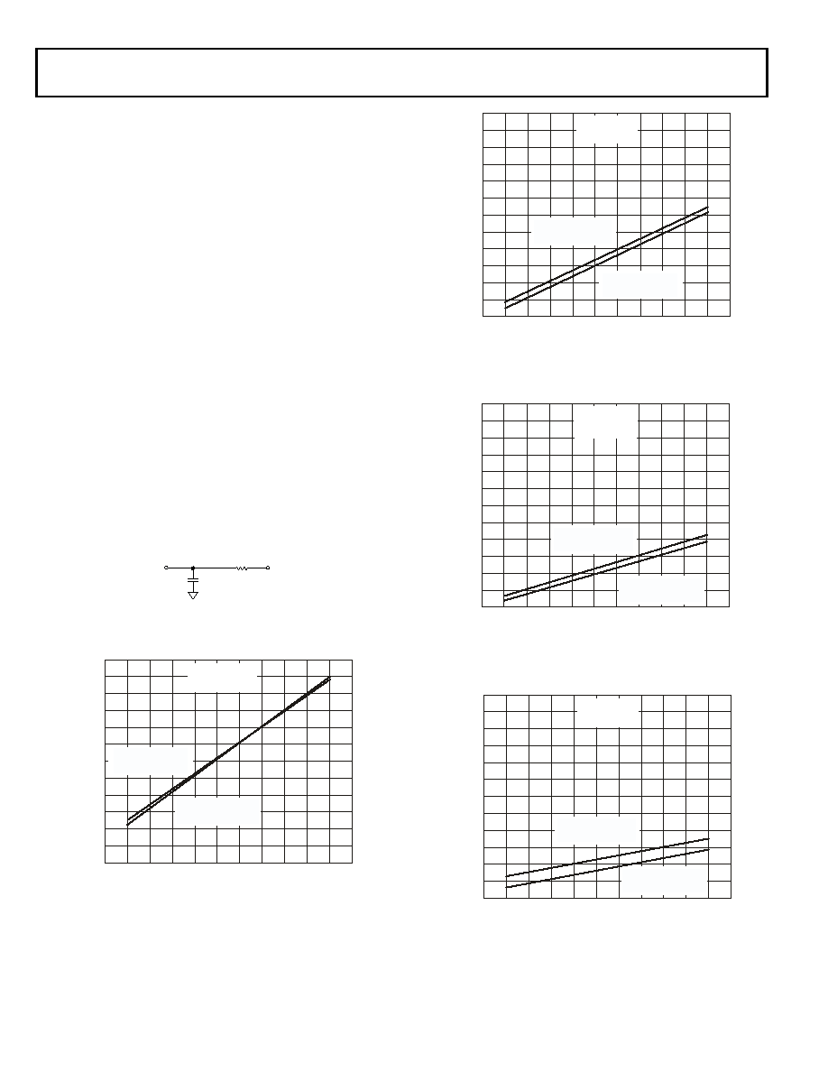
Capacitive Loading
Output valid and hold are based on standard capacitive loads:
30 pF on all pins (see Figure 36). The delay and hold specifica-
tions given should be derated by a drive strength related factor
for loads other than the nominal value of 30 pF. Figure 37
through Figure 44 show how output rise time varies with capac-
itance. Figure 45 graphically shows how output valid varies with
load capacitance. (Note that this graph or derating does not
apply to output disable delays; see Output Disable Time on
linear outside the ranges shown.
Figure 36. Equivalent Device Loading for AC Measurements
(Includes All Fixtures)
Figure 37. Typical Output Rise and Fall Time (10% to 90%, VDD_IO =2.5 V)
vs. Load Capacitance at Strength 0
tRAMP
CL V
Δ
() I
D
=
1.25V
TO
OUTPUT
PIN
30pF
50
0
10
20
30
40
50
60
70
80
90
100
0
5
10
15
20
25
RISE TIME
Y = 0.259x + 3.0842
STRENGTH 0
(VDD_IO =2.5V)
R
IS
E
A
N
D
F
A
L
T
IM
E
S
(n
s
)
LOAD CAPACITANCE (pF)
FALL TIME
Y = 0.251x + 4.2245
Figure 38. Typical Output Rise and Fall Time (10% to 90%, VDD_IO =2.5 V)
vs. Load Capacitance at Strength 1
Figure 39. Typical Output Rise and Fall Time (10% to 90%, VDD_IO =2.5 V)
vs. Load Capacitance at Strength 2
Figure 40. Typical Output Rise and Fall Time (10% to 90%, VDD_IO =2.5 V)
vs. Load Capacitance at Strength 3
0
10
20
30
405060
70
80
90
100
0
5
10
15
20
25
R
IS
E
A
N
D
F
A
L
T
IM
E
S
(n
s
)
LOAD CAPACITANCE (pF)
STRENGTH 1
(VDD_IO =2.5V)
RISE TIME
Y = 0.1501
x +0.05
FALL TIME
Y = 0.1527x + 0.7485
0
102030
40
50
60
70
80
90
100
0
5
10
15
20
25
R
IS
E
A
N
D
F
A
L
T
IM
E
S
(n
s
)
LOAD CAPACITANCE (pF)
STRENGTH 2
(VDD_IO =2.5V)
RISE TIME
Y = 0.0861
x + 0.4712
FALL TIME
Y = 0.0949x + 0.8112
0
102030
40
50
60
7080
90
100
0
5
10
15
20
25
R
IS
E
A
N
D
F
A
L
T
IM
E
S
(n
s
)
LOAD CAPACITANCE (pF)
STRENGTH 3
(VDD_IO =2.5V)
RISE TIME
Y= 0.06
x +1.1362
FALL TIME
Y = 0.0691x + 1.1158
相关PDF资料 |
PDF描述 |
|---|---|
| ADSP-TS101SAB2-100 | IC DSP CONTROLLER 6MBIT 484 BGA |
| VE-B34-CY-S | CONVERTER MOD DC/DC 48V 50W |
| ATFC-0402-1N0-BT | INDUCTOR THIN FILM 1.0NH 0402 |
| ADSP-TS201SABPZ050 | IC PROCESSOR 500MHZ 576BGA |
| TAJY475M050RNJ | CAP TANT 4.7UF 50V 20% 2917 |
相关代理商/技术参数 |
参数描述 |
|---|---|
| ADSP-TS201SABP-060 | 功能描述:IC PROCESSOR 600MHZ 576BGA RoHS:否 类别:集成电路 (IC) >> 嵌入式 - DSP(数字式信号处理器) 系列:TigerSHARC® 标准包装:2 系列:StarCore 类型:SC140 内核 接口:DSI,以太网,RS-232 时钟速率:400MHz 非易失内存:外部 芯片上RAM:1.436MB 电压 - 输入/输出:3.30V 电压 - 核心:1.20V 工作温度:-40°C ~ 105°C 安装类型:表面贴装 封装/外壳:431-BFBGA,FCBGA 供应商设备封装:431-FCPBGA(20x20) 包装:托盘 |
| ADSP-TS201SABP-10X | 制造商:Analog Devices 功能描述: |
| ADSP-TS201SABP-15X | 制造商:Analog Devices 功能描述: |
| ADSP-TS201SABP-ENG | 制造商:Analog Devices 功能描述: |
| ADSP-TS201SABP-ENG1 | 制造商:Analog Devices 功能描述: |
发布紧急采购,3分钟左右您将得到回复。