- 您现在的位置:买卖IC网 > PDF目录19370 > ADSP-TS201SABP-050 (Analog Devices Inc)IC PROCESSOR 500MHZ 576BGA PDF资料下载
参数资料
| 型号: | ADSP-TS201SABP-050 |
| 厂商: | Analog Devices Inc |
| 文件页数: | 22/48页 |
| 文件大小: | 0K |
| 描述: | IC PROCESSOR 500MHZ 576BGA |
| 标准包装: | 1 |
| 系列: | TigerSHARC® |
| 类型: | 定点/浮点 |
| 接口: | 主机接口,连接端口,多处理器 |
| 时钟速率: | 500MHz |
| 非易失内存: | 外部 |
| 芯片上RAM: | 3MB |
| 电压 - 输入/输出: | 2.50V |
| 电压 - 核心: | 1.05V |
| 工作温度: | -40°C ~ 85°C |
| 安装类型: | 表面贴装 |
| 封装/外壳: | 576-BBGA 裸露焊盘 |
| 供应商设备封装: | 576-BGA-ED(25x25) |
| 包装: | 托盘 |
| 配用: | ADZS-TS201S-EZLITE-ND - KIT LITE EVAL FOR ADSP-TS201S |
第1页第2页第3页第4页第5页第6页第7页第8页第9页第10页第11页第12页第13页第14页第15页第16页第17页第18页第19页第20页第21页当前第22页第23页第24页第25页第26页第27页第28页第29页第30页第31页第32页第33页第34页第35页第36页第37页第38页第39页第40页第41页第42页第43页第44页第45页第46页第47页第48页
ADSP-TS201S
Rev. C
|
Page 29 of 48
|
December 2006
DS2–08
Static Pins—Must Be Constant
—
SCLKRAT2–08
Static Pins—Must Be Constant
—
ENEDREG
Static Pins—Must Be Connected to VSS
——
—
STRAP SYS
9, 10
Strap Pins
1.5
0.5
——
SCLK
JTAG SYS
11, 12
JTAG System Pins
+2.5
+10.0
+12.0
–1.0
—
TCK
1 The external port protocols employ bus IDLE cycles for bus mastership transitions as well as slave access boundary crossings to avoid any potential bus contention. The
apparent driver overlap, due to output disables being larger than output enables, is not actual.
2 For input specifications on FLAG3–0 pins, see Table 21.
3 These input pins are asynchronous and therefore do not need to be synchronized to a clock reference.
4 For additional requirement details, see Reset and Booting on Page 9.
5 RST_IN clock reference is the falling edge of SCLK.
6 TDO output clock reference is the falling edge of TCK.
7 Reference clock depends on function.
8 These pins may change only during reset; recommend connecting it to VDD_IO/VSS.
9 STRAP pins include: BMS, BM, BUSLOCK, TMR0E, L1BCMPO, L2BCMPO, and L3BCMPO.
10Specifications applicable during reset only.
11JTAG system pins include: RST_IN, RST_OUT, POR_IN, IRQ3–0, DMAR3–0, HBR, BOFF, MS1–0, MSH, SDCKE, LDQM, HDQM, BMS, IOWR, IORD, BM, EMU, SDA10,
IOEN, BUSLOCK, TMR0E, DATA63–0, ADDR31–0, RD, WRL, WRH, BRST, MSSD3–0, RAS, CAS, SDWE, HBG, BR7–0, FLAG3–0, L0DATOP3–0, L0DATON3–0,
L1DATOP3–0, L1DATON3–0, L2DATOP3–0, L2DATON3–0, L3DATOP3–0, L3DATON3–0, L0CLKOUTP, L0CLKOUTN, L1CLKOUTP, L1CLKOUTN, L2CLKOUTP,
L2CLKOUTN, L3CLKOUTP, L3CLKOUTN, L0ACKI, L1ACKI, L2ACKI, L3ACKI, L0DATIP3–0, L0DATIN3–0, L1DATIP3–0, L1DATIN3–0, L2DATIP3–0,
L2DATIN3–0, L3DATIP3–0, L3DATIN3–0, L0CLKINP, L0CLKINN, L1CLKINP, L1CLKINN, L2CLKINP, L2CLKINN, L3CLKINP, L3CLKINN, L0ACKO, L1ACKO,
L2ACKO, L3ACKO, ACK, CPA, DPA, L0BCMPO, L1BCMPO, L2BCMPO, L3BCMPO, L0BCMPI, L1BCMPI, L2BCMPI, L3BCMPI, ID2–0, CTRL_IMPD1–0,
SCLKRAT2–0, DS2–0, ENEDREG.
12JTAG system output timing clock reference is the falling edge of TCK.
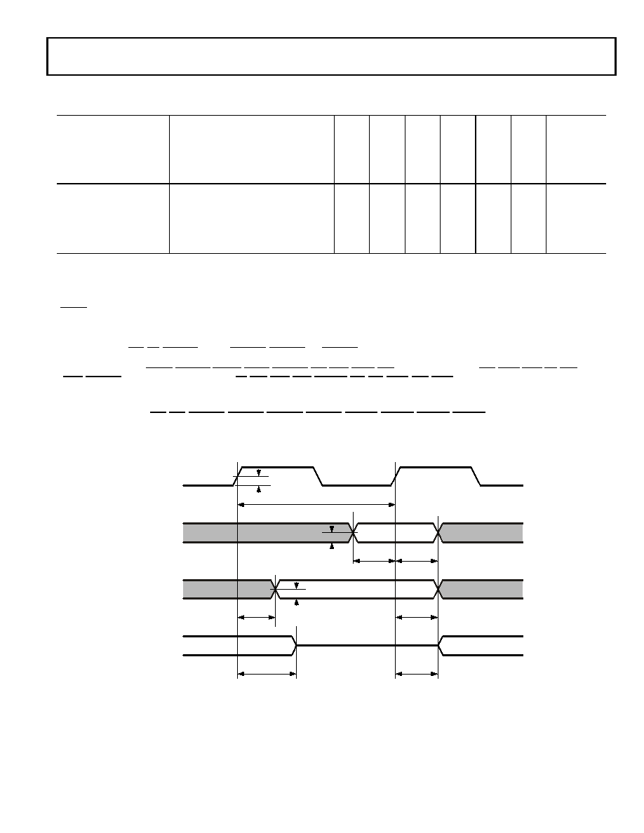
Figure 15. General AC Parameters Timing
Table 29. AC Signal Specifications (Continued)
(All values in this table are in nanoseconds.)
Name
Description
In
put
S
e
tu
p
(M
in
)
In
put
Hold
(M
in
)
Ou
tp
u
tV
a
li
d
(M
a
x
)
Ou
tp
u
tH
o
ld
(M
in
)
Ou
tp
u
tEn
ab
le
(M
in
)1
Ou
tpu
tDi
sab
le
(M
a
x
)1
Re
fe
re
nce
Cl
ock
REFERENCE
CLOCK
INPUT
SIGNAL
OUTPUT
SIGNAL
THREE-
STATE
OUTPUT
VALID
OUTPUT
HOLD
OUTPUT
ENABLE
OUTPUT
DISABLE
INPUT
HOLD
INPUT
SETUP
1.25V
tSCLK OR tTCK
相关PDF资料 |
PDF描述 |
|---|---|
| ADSP-TS101SAB2-100 | IC DSP CONTROLLER 6MBIT 484 BGA |
| VE-B34-CY-S | CONVERTER MOD DC/DC 48V 50W |
| ATFC-0402-1N0-BT | INDUCTOR THIN FILM 1.0NH 0402 |
| ADSP-TS201SABPZ050 | IC PROCESSOR 500MHZ 576BGA |
| TAJY475M050RNJ | CAP TANT 4.7UF 50V 20% 2917 |
相关代理商/技术参数 |
参数描述 |
|---|---|
| ADSP-TS201SABP-060 | 功能描述:IC PROCESSOR 600MHZ 576BGA RoHS:否 类别:集成电路 (IC) >> 嵌入式 - DSP(数字式信号处理器) 系列:TigerSHARC® 标准包装:2 系列:StarCore 类型:SC140 内核 接口:DSI,以太网,RS-232 时钟速率:400MHz 非易失内存:外部 芯片上RAM:1.436MB 电压 - 输入/输出:3.30V 电压 - 核心:1.20V 工作温度:-40°C ~ 105°C 安装类型:表面贴装 封装/外壳:431-BFBGA,FCBGA 供应商设备封装:431-FCPBGA(20x20) 包装:托盘 |
| ADSP-TS201SABP-10X | 制造商:Analog Devices 功能描述: |
| ADSP-TS201SABP-15X | 制造商:Analog Devices 功能描述: |
| ADSP-TS201SABP-ENG | 制造商:Analog Devices 功能描述: |
| ADSP-TS201SABP-ENG1 | 制造商:Analog Devices 功能描述: |
发布紧急采购,3分钟左右您将得到回复。