- 您现在的位置:买卖IC网 > PDF目录1900 > ADUC7039BCP6Z-RL (Analog Devices Inc)IC MCU ARM7 BATT SENSER 32LFCSP PDF资料下载
参数资料
| 型号: | ADUC7039BCP6Z-RL |
| 厂商: | Analog Devices Inc |
| 文件页数: | 17/92页 |
| 文件大小: | 0K |
| 描述: | IC MCU ARM7 BATT SENSER 32LFCSP |
| 标准包装: | 2,500 |
| 系列: | MicroConverter® ADuC7xxx |
| 核心处理器: | ARM7 |
| 芯体尺寸: | 16/32-位 |
| 速度: | 20.48MHz |
| 连通性: | LIN,SPI |
| 外围设备: | POR,温度传感器,WDT |
| 输入/输出数: | 6 |
| 程序存储器容量: | 64KB(32K x 16) |
| 程序存储器类型: | 闪存 |
| RAM 容量: | 1K x 32 |
| 电压 - 电源 (Vcc/Vdd): | 3.5 V ~ 18 V |
| 数据转换器: | A/D 2x16b |
| 振荡器型: | 内部 |
| 工作温度: | -40°C ~ 115°C |
| 封装/外壳: | 32-VFQFN 裸露焊盘,CSP |
| 包装: | 带卷 (TR) |
第1页第2页第3页第4页第5页第6页第7页第8页第9页第10页第11页第12页第13页第14页第15页第16页当前第17页第18页第19页第20页第21页第22页第23页第24页第25页第26页第27页第28页第29页第30页第31页第32页第33页第34页第35页第36页第37页第38页第39页第40页第41页第42页第43页第44页第45页第46页第47页第48页第49页第50页第51页第52页第53页第54页第55页第56页第57页第58页第59页第60页第61页第62页第63页第64页第65页第66页第67页第68页第69页第70页第71页第72页第73页第74页第75页第76页第77页第78页第79页第80页第81页第82页第83页第84页第85页第86页第87页第88页第89页第90页第91页第92页
ADuC7039
Data Sheet
Rev. D | Page 24 of 92
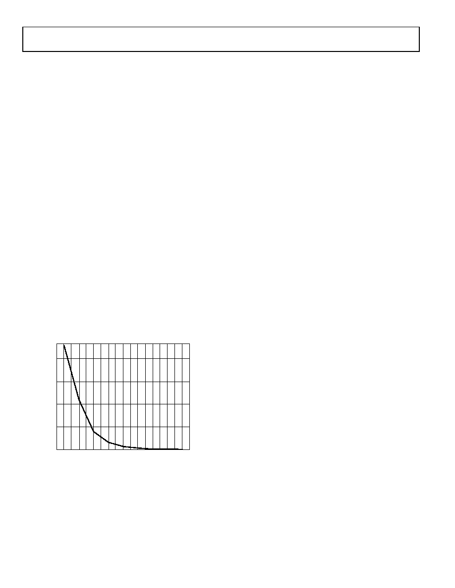
FLASH/EE MEMORY RELIABILITY
The Flash/EE memory array on the part is fully qualified for
two key Flash/EE memory characteristics: Flash/EE memory
cycling endurance and Flash/EE memory data retention.
Endurance quantifies the ability of the Flash/EE memory to be
cycled through many program, read, and erase cycles. A single
endurance cycle is composed of four independent, sequential
events, defined as
Initial page erase sequence.
Read/verify sequence.
Byte program sequence.
Second read/verify sequence.
In reliability qualification, every half-word (16-bit wide) loca-
tion of the three pages (top, middle, and bottom) in the Flash/EE
memory is cycled 10,000 times from 0x0000 to 0xFFFF. As
indicated in Table 1, the Flash/EE memory endurance qualifi-
cation of the part is carried out in accordance with the JEDEC
Retention Lifetime Specification A117. The results allow the
specification of a minimum endurance figure over supply and
temperature of 10,000 cycles.
Retention quantifies the ability of the Flash/EE memory to
retain its programmed data over time. The part is qualified in
accordance with the formal JEDEC Retention Lifetime Specifi-
cation A117 at a specific junction temperature (TJ = 85°C) as
indicated in Table 1. This means that the Flash/EE memory
is guaranteed to retain its data for its fully specified retention
lifetime every time the Flash/EE memory is reprogrammed.
Also, note that retention lifetime, based on an activation energy
Figure 8. Flash/EE Memory Data Retention
ADuC7039 KERNEL
The ADuC7039 features an on-chip kernel resident in the
top 2 kB of the Flash/EE code space. After any reset event,
this kernel calculates its own checksum and compares it to the
checksum programmed during production test, to ensure that
the kernel does not contain any error. If an error occurs, the
SYSCHK register contains its default value and user mode is
entered. In normal circumstances, the checksum is written to
the SYSCHK MMR.
System Kernel Checksum
Name:
SYSCHK
Address:
0xFFFF0244
Default Value: 0x00000000 (updated by kernel at power-on)
Access:
Read/write
Function:
At power-on, this 32-bit register holds the
kernel checksum.
The kernel then copies the factory calibrated data from the
manufacturing data space into the various on-chip peripherals.
The peripherals calibrated by the kernel are as follows:
Precision oscillator
Low power oscillator
REG_AVDD/REG_DVDD
Voltage reference
Current ADC (offset and gain)
Voltage/temperature ADC (offset and gain)
Processor registers and user registers that can be modified
by the kernel and differ from their POR default values are as
follows:
R0 to R15
GP0CON
SYSCHK
FEEADR/FEEDAT/FEECON/FEESIG
HVDAT/HVCON
HVCFG
T2LD
The ADuC7039 also features an on-chip LIN downloader.
A flow chart of the execution of the kernel is shown in Figure 9.
The current revision of the kernel can be derived from R5, as
described in Table 66.
After any reset, the watchdog timer is disabled once the kernel
code is exited. For the duration of the kernel execution, the
watchdog timer is active with a timeout period of 500 ms. This
ensures that if an error occurs in the kernel, the ADuC7039
automatically resets. If LIN download mode is entered, the
watchdog is periodically refreshed.
0
150
300
450
600
30
40
55
70
85
100
125
135
150
RE
T
E
NT
IO
N
(
Y
ears)
JUNCTION TEMPERATURE (°C)
08463-
009
相关PDF资料 |
PDF描述 |
|---|---|
| ADUC7061BCPZ32 | IC MCU 16/32BIT 32KB 32LFCSP |
| ADUC7121BBCZ-RL | PRECISION ANALOG MCU I.C |
| ADUC7122BBCZ-RL | PRECISION ANALOG MCU I.C |
| ADUC7126BSTZ126-RL | IC MCU 16/32B 126KB FLASH 80LQFP |
| ADUC7129BSTZ126 | IC DAS MCU ARM7 ADC/DDS 80-LQFP |
相关代理商/技术参数 |
参数描述 |
|---|---|
| ADUC7039WBCPZ | 制造商:Analog Devices 功能描述:FLASH 64K ARM7 DUAL 16-BIT ADC LIN I.C. - Trays 制造商:Analog Devices 功能描述:IC MCU ARM7 64KB FLASH 32LFCSP 制造商:Analog Devices 功能描述:Flash 64k ARM7 Dual 16-Bit ADC LIN I.C. |
| ADUC7039WBCPZ-RL | 制造商:Analog Devices 功能描述:FLASH 64K ARM7 DUAL 16-BIT ADC LIN I.C. - Tape and Reel 制造商:Analog Devices 功能描述:IC MCU ARM7 64KB FLASH 32LFCSP 制造商:Analog Devices 功能描述:Flash 64k ARM7 Dual 16-Bit ADC LIN I.C. |
| ADUC7060 | 制造商:AD 制造商全称:Analog Devices 功能描述:Low Power, Precision Analog Microcontroller, Dual Sigma-Delta ADCs, Flash/EE, ARM7TDMI |
| ADUC7060BCPZ32 | 功能描述:IC MCU 24BIT 32KB FLASH 48LFCSP RoHS:是 类别:集成电路 (IC) >> 嵌入式 - 微控制器, 系列:MicroConverter® ADuC7xxx 产品培训模块:MCU Product Line Introduction XMEGA Introduction AVR XMEGA USB Connectivity 标准包装:90 系列:AVR® XMEGA 核心处理器:AVR 芯体尺寸:8/16-位 速度:32MHz 连通性:I²C,IrDA,SPI,UART/USART 外围设备:欠压检测/复位,DMA,POR,PWM,WDT 输入/输出数:50 程序存储器容量:192KB(96K x 16) 程序存储器类型:闪存 EEPROM 大小:4K x 8 RAM 容量:16K x 8 电压 - 电源 (Vcc/Vdd):1.6 V ~ 3.6 V 数据转换器:A/D 16x12b; D/A 2x12b 振荡器型:内部 工作温度:-40°C ~ 85°C 封装/外壳:64-TQFP 包装:托盘 配用:ATSTK600-RC14-ND - STK600 SOCKET/ADAPTER 64TQFPATSTK600-TQFP64-ND - STK600 SOCKET/ADAPTER 64-TQFPATAVRONEKIT-ND - KIT AVR/AVR32 DEBUGGER/PROGRMMRATAVRISP2-ND - PROGRAMMER AVR IN SYSTEM |
| ADUC7060BCPZ32-RL | 功能描述:IC MCU FLASH 24BIT 32KB 48LFCSP RoHS:是 类别:集成电路 (IC) >> 嵌入式 - 微控制器, 系列:MicroConverter® ADuC7xxx 标准包装:38 系列:Encore!® XP® 核心处理器:eZ8 芯体尺寸:8-位 速度:5MHz 连通性:IrDA,UART/USART 外围设备:欠压检测/复位,LED,POR,PWM,WDT 输入/输出数:16 程序存储器容量:4KB(4K x 8) 程序存储器类型:闪存 EEPROM 大小:- RAM 容量:1K x 8 电压 - 电源 (Vcc/Vdd):2.7 V ~ 3.6 V 数据转换器:- 振荡器型:内部 工作温度:-40°C ~ 105°C 封装/外壳:20-SOIC(0.295",7.50mm 宽) 包装:管件 其它名称:269-4116Z8F0413SH005EG-ND |
发布紧急采购,3分钟左右您将得到回复。