- 您现在的位置:买卖IC网 > PDF目录11208 > ADUC7060BCPZ32-RL (Analog Devices Inc)IC MCU FLASH 24BIT 32KB 48LFCSP PDF资料下载
参数资料
| 型号: | ADUC7060BCPZ32-RL |
| 厂商: | Analog Devices Inc |
| 文件页数: | 37/108页 |
| 文件大小: | 0K |
| 描述: | IC MCU FLASH 24BIT 32KB 48LFCSP |
| 设计资源: | 4 mA-to-20 mA Loop-Powered Temperature Monitor Using ADuC7060/1 (CN0145) Low power, Long Range, ISM Wireless Measuring Node (CN0164) |
| 标准包装: | 2,500 |
| 系列: | MicroConverter® ADuC7xxx |
| 核心处理器: | ARM7 |
| 芯体尺寸: | 16/32-位 |
| 速度: | 10MHz |
| 连通性: | I²C,SPI,UART/USART |
| 外围设备: | POR,PWM,温度传感器,WDT |
| 输入/输出数: | 14 |
| 程序存储器容量: | 32KB(16K x 16) |
| 程序存储器类型: | 闪存 |
| RAM 容量: | 1K x 32 |
| 电压 - 电源 (Vcc/Vdd): | 2.375 V ~ 2.625 V |
| 数据转换器: | A/D 5x24b,8x24b,D/A 1x14b |
| 振荡器型: | 内部 |
| 工作温度: | -40°C ~ 125°C |
| 封装/外壳: | 48-VFQFN 裸露焊盘,CSP |
| 包装: | 带卷 (TR) |
第1页第2页第3页第4页第5页第6页第7页第8页第9页第10页第11页第12页第13页第14页第15页第16页第17页第18页第19页第20页第21页第22页第23页第24页第25页第26页第27页第28页第29页第30页第31页第32页第33页第34页第35页第36页当前第37页第38页第39页第40页第41页第42页第43页第44页第45页第46页第47页第48页第49页第50页第51页第52页第53页第54页第55页第56页第57页第58页第59页第60页第61页第62页第63页第64页第65页第66页第67页第68页第69页第70页第71页第72页第73页第74页第75页第76页第77页第78页第79页第80页第81页第82页第83页第84页第85页第86页第87页第88页第89页第90页第91页第92页第93页第94页第95页第96页第97页第98页第99页第100页第101页第102页第103页第104页第105页第106页第107页第108页
ADuC7060/ADuC7061
Data Sheet
Rev. D | Page 34 of 108
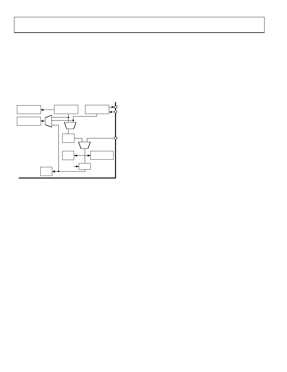
OSCILLATOR, PLL, AND POWER CONTROL
CLOCKING SYSTEM
The ADuC706x integrates a 32.768 kHz ±3% oscillator, a clock
divider, and a PLL. The PLL locks onto a multiple of the inter-
nal oscillator or an external 32.768 kHz crystal to provide a stable
10.24 MHz clock (UCLK) for the system. To allow power saving,
the core can operate at this frequency or at binary submultiples
of it. The actual core operating frequency, UCLK/2CD, is refered
to as HCLK. The default core clock is the PLL clock divided by 8
(CD = 3) or 1.28 MHz.
PLL
CORE
CD
10.24MHz
32.768kHz
*32.768kHz ±3%
HCLK
UCLK
OCLK
WATCHDOG
TIMER
WAKE-UP
TIMER
INT. 32kHz
OSCILLATOR*
CRYSTAL
OSCILLATOR
XCLKO
XCLKI
ANALOG
PERIPHERALS
/2CD
I2C
07079-
008
P2.0/EXTCLK
Figure 13. Clocking System
External Crystal Selection
To switch to an external crystal, users must follow this procedure:
1. Enable the Timer1 interrupt and configure it for a timeout
period of >120 s.
2. Follow the write sequence to the PLLCON register, setting the
OSEL bits to [10] and clearing the EXTCLK bit.
3. Force the part into nap mode by following the correct write
sequence to the POWCON register.
4. When the part is interrupted from nap mode by the Timer1
interrupt source, the clock source has switched to the external
crystal.
Example source code
T1LD
= 0x80;
// 32,768 clock ticks
T1CON = 0xC0;
// Periodic mode, enable
// timer, 32,768 Hz clock/1
IRQEN |= 0x10; // Enable Timer1 interrupt
// source
PLLKEY1 = 0xAA;
// Switch to external crystal
PLLCON = 0x2;
PLLKEY2 = 0x55;
POWKEY1 = 0x1;
// Enter nap mode
POWCON0 = 0x73;
POWKEY2 = 0xF4;
In case of crystal loss, the watchdog timer should be used. During
initialization, a test on the RSTSTA can determine if the reset came
from the watchdog timer.
External Clock Selection
To switch to an external clock on P2.0, configure P2.0 in Mode 0.
The external clock can be up to 20.48 MHz, provided that the toler-
ance is 1%. The external clock is divided by 2 internally on the part.
Example source code
T1LD
= 0x80;
T1CON = 0xC0;
IRQEN |= 0x10;
// Enable Timer1 interrupt
PLLKEY1 = 0xAA;
// Switch to external clock
PLLCON = 0x4;
PLLKEY2 = 0x55;
POWKEY1 = 0x1;
// Enter NAP mode
POWCON0 = 0x73;
POWKEY2 = 0xF4;
The selection of the clock source is in the PLLCON register. By
default, the part uses the internal oscillator feeding the PLL.
POWER CONTROL SYSTEM
The core clock frequency is changed by writing to the POWCON0
register. This is a key protected register; therefore, Register POWKEY1
and Register POWKEY2 must be written to immediately before and
after configuring the POWCON0 register. The following is a simple
example showing how to configure the core clock for 10.24 MHz:
POWKEY1 = 0x1;
POWCON0 = 0x78;
//Set core to max CPU
//speed of 10.24 MHz
POWKEY2 = 0xF4;
A choice of operating modes is available on the ADuC706x. Table 33
describes what part is powered on in the different modes and
indicates the power-up time.
Table 34 gives some typical values for the total current consumption
(analog + digital supply currents) in the different modes, depending
on the clock divider bits. The ADC is turned off. Note that these
values also include the current consumption of the regulator and
other parts on the test board where these values are measured.
相关PDF资料 |
PDF描述 |
|---|---|
| AD7510DIKQ | IC SWITCH QUAD SPST 16CDIP |
| LX256EV-5FN484I | IC SWITCH DIGITAL 484FPBGA |
| LX256EV-35FN484C | IC SWITCH DIGITAL 484FPBGA |
| LX256V-5FN484C | IC SWITCH DIGITAL 484FPBGA |
| ATSAM3U1CB-CU | IC MCU 64KB CORTEX-M3 100-TFBGA |
相关代理商/技术参数 |
参数描述 |
|---|---|
| ADUC7060BSTZ32 | 功能描述:IC MCU FLASH 24BIT 32KB 48LQFP RoHS:是 类别:集成电路 (IC) >> 嵌入式 - 微控制器, 系列:MicroConverter® ADuC7xxx 产品培训模块:MCU Product Line Introduction XMEGA Introduction AVR XMEGA USB Connectivity 标准包装:90 系列:AVR® XMEGA 核心处理器:AVR 芯体尺寸:8/16-位 速度:32MHz 连通性:I²C,IrDA,SPI,UART/USART 外围设备:欠压检测/复位,DMA,POR,PWM,WDT 输入/输出数:50 程序存储器容量:192KB(96K x 16) 程序存储器类型:闪存 EEPROM 大小:4K x 8 RAM 容量:16K x 8 电压 - 电源 (Vcc/Vdd):1.6 V ~ 3.6 V 数据转换器:A/D 16x12b; D/A 2x12b 振荡器型:内部 工作温度:-40°C ~ 85°C 封装/外壳:64-TQFP 包装:托盘 配用:ATSTK600-RC14-ND - STK600 SOCKET/ADAPTER 64TQFPATSTK600-TQFP64-ND - STK600 SOCKET/ADAPTER 64-TQFPATAVRONEKIT-ND - KIT AVR/AVR32 DEBUGGER/PROGRMMRATAVRISP2-ND - PROGRAMMER AVR IN SYSTEM |
| ADUC7060BSTZ32-RL | 功能描述:IC ARM7 MCU FLASH 32K 48LQFP RoHS:是 类别:集成电路 (IC) >> 嵌入式 - 微控制器, 系列:MicroConverter® ADuC7xxx 标准包装:38 系列:Encore!® XP® 核心处理器:eZ8 芯体尺寸:8-位 速度:5MHz 连通性:IrDA,UART/USART 外围设备:欠压检测/复位,LED,POR,PWM,WDT 输入/输出数:16 程序存储器容量:4KB(4K x 8) 程序存储器类型:闪存 EEPROM 大小:- RAM 容量:1K x 8 电压 - 电源 (Vcc/Vdd):2.7 V ~ 3.6 V 数据转换器:- 振荡器型:内部 工作温度:-40°C ~ 105°C 封装/外壳:20-SOIC(0.295",7.50mm 宽) 包装:管件 其它名称:269-4116Z8F0413SH005EG-ND |
| ADUC7061BCPZ32 | 功能描述:IC MCU 16/32BIT 32KB 32LFCSP RoHS:是 类别:集成电路 (IC) >> 嵌入式 - 微控制器, 系列:MicroConverter® ADuC7xxx 标准包装:38 系列:Encore!® XP® 核心处理器:eZ8 芯体尺寸:8-位 速度:5MHz 连通性:IrDA,UART/USART 外围设备:欠压检测/复位,LED,POR,PWM,WDT 输入/输出数:16 程序存储器容量:4KB(4K x 8) 程序存储器类型:闪存 EEPROM 大小:- RAM 容量:1K x 8 电压 - 电源 (Vcc/Vdd):2.7 V ~ 3.6 V 数据转换器:- 振荡器型:内部 工作温度:-40°C ~ 105°C 封装/外壳:20-SOIC(0.295",7.50mm 宽) 包装:管件 其它名称:269-4116Z8F0413SH005EG-ND |
| ADUC7061BCPZ32-RL | 功能描述:IC MCU 16/32BIT 32KB 32LFCSP RoHS:是 类别:集成电路 (IC) >> 嵌入式 - 微控制器, 系列:MicroConverter® ADuC7xxx 标准包装:38 系列:Encore!® XP® 核心处理器:eZ8 芯体尺寸:8-位 速度:5MHz 连通性:IrDA,UART/USART 外围设备:欠压检测/复位,LED,POR,PWM,WDT 输入/输出数:16 程序存储器容量:4KB(4K x 8) 程序存储器类型:闪存 EEPROM 大小:- RAM 容量:1K x 8 电压 - 电源 (Vcc/Vdd):2.7 V ~ 3.6 V 数据转换器:- 振荡器型:内部 工作温度:-40°C ~ 105°C 封装/外壳:20-SOIC(0.295",7.50mm 宽) 包装:管件 其它名称:269-4116Z8F0413SH005EG-ND |
| ADUC70SMARTLINKRL7 | 制造商:Analog Devices 功能描述: |
发布紧急采购,3分钟左右您将得到回复。