- 您现在的位置:买卖IC网 > PDF目录11208 > ADUC7060BCPZ32-RL (Analog Devices Inc)IC MCU FLASH 24BIT 32KB 48LFCSP PDF资料下载
参数资料
| 型号: | ADUC7060BCPZ32-RL |
| 厂商: | Analog Devices Inc |
| 文件页数: | 62/108页 |
| 文件大小: | 0K |
| 描述: | IC MCU FLASH 24BIT 32KB 48LFCSP |
| 设计资源: | 4 mA-to-20 mA Loop-Powered Temperature Monitor Using ADuC7060/1 (CN0145) Low power, Long Range, ISM Wireless Measuring Node (CN0164) |
| 标准包装: | 2,500 |
| 系列: | MicroConverter® ADuC7xxx |
| 核心处理器: | ARM7 |
| 芯体尺寸: | 16/32-位 |
| 速度: | 10MHz |
| 连通性: | I²C,SPI,UART/USART |
| 外围设备: | POR,PWM,温度传感器,WDT |
| 输入/输出数: | 14 |
| 程序存储器容量: | 32KB(16K x 16) |
| 程序存储器类型: | 闪存 |
| RAM 容量: | 1K x 32 |
| 电压 - 电源 (Vcc/Vdd): | 2.375 V ~ 2.625 V |
| 数据转换器: | A/D 5x24b,8x24b,D/A 1x14b |
| 振荡器型: | 内部 |
| 工作温度: | -40°C ~ 125°C |
| 封装/外壳: | 48-VFQFN 裸露焊盘,CSP |
| 包装: | 带卷 (TR) |
第1页第2页第3页第4页第5页第6页第7页第8页第9页第10页第11页第12页第13页第14页第15页第16页第17页第18页第19页第20页第21页第22页第23页第24页第25页第26页第27页第28页第29页第30页第31页第32页第33页第34页第35页第36页第37页第38页第39页第40页第41页第42页第43页第44页第45页第46页第47页第48页第49页第50页第51页第52页第53页第54页第55页第56页第57页第58页第59页第60页第61页当前第62页第63页第64页第65页第66页第67页第68页第69页第70页第71页第72页第73页第74页第75页第76页第77页第78页第79页第80页第81页第82页第83页第84页第85页第86页第87页第88页第89页第90页第91页第92页第93页第94页第95页第96页第97页第98页第99页第100页第101页第102页第103页第104页第105页第106页第107页第108页
Data Sheet
ADuC7060/ADuC7061
Rev. D | Page 57 of 108
DAC0DAT Register
Name:
DAC0DAT
Address:
0xFFFF0604
Default value: 0x00000000
Access:
Read and write
Function:
This 32-bit MMR contains the DAC output
value.
Table 64. DAC0DAT MMR Bit Designations
Bit
Description
31:28
Reserved.
27:16
12-bit data for DAC0.
15:12
Extra four bits used in interpolation mode.
11:0
Reserved.
USING THE DAC
The on-chip DAC architecture consists of a resistor string DAC
followed by an output buffer amplifier.
The reference source for the DAC is user selectable in software. It
can be AVDD, VREF±, or ADCx/EXT_REF2IN±.
In 0-to-AVDD mode, the DAC output transfer function
spans from 0 V to the voltage at the AVDD pin.
In VREF± and ADCx/EXT_REF2IN± modes, the DAC
output transfer function spans from negative input voltage
to the voltage positive input pin. Note that these voltages
must never go below 0 V or above AVDD.
In 0-to-VREF mode, the DAC output transfer function spans
from 0 V to the internal 1.2 V reference, VREF.
The DAC can be configured in three different user modes:
normal mode, DAC interpolation mode, and op amp mode.
Normal DAC Mode
In this mode of operation, the DAC is configured as a 12-bit
voltage output DAC. By default, the DAC buffer is enabled, but
the output buffer can be disabled. If the DAC output buffer is
disabled, the DAC is capable of driving a capacitive load of only
20 pF. The DAC buffer is disabled by setting the DACBUFBYPASS
bit in DAC0CON.
The DAC output buffer amplifier features a true, rail-to-rail
output stage implementation. This means that when unloaded,
each output is capable of swinging to within less than 5 mV of
both AVDD and ground. Moreover, the linearity specification of
the DAC (when driving a 5 kΩ resistive load to ground) is guar-
anteed through the full transfer function except for Code 0
to Code 100 and, in 0-to- AVDD mode only, Code 3995 to
Code 4095. Linearity degradation near ground and AVDD is
caused by saturation of the output amplifier, and a general
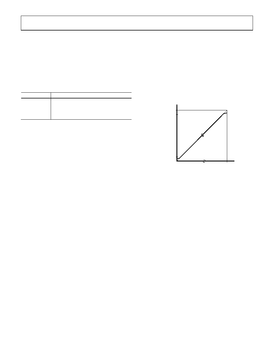
representation of its effects (neglecting offset and gain error) is
illustrated in Figure 21. The dotted line in Figure 21 indicates the
ideal transfer function, and the solid line represents what the
transfer function may look like with endpoint nonlinearities due
to saturation of the output amplifier. Note that Figure 21 repre-
sents a transfer function in 0-to-AVDD mode only. In 0-to-VREF
or, VREF±, and ADCx/EXT_REF2IN± modes (with VREF < AVDD
or ADCx/EXT_REF2IN± < AVDD), the lower nonlinearity is
similar. However, the upper portion of the transfer function
follows the ideal line all the way to the end (VREF in this case, not
AVDD), showing no signs of endpoint linearity errors.
AVDD
AVDD – 100mV
100mV
0x00000000
0x0FFF0000
07079-
015
Figure 21. Endpoint Nonlinearities Due to Amplifier Saturation
The endpoint nonlinearities conceptually illustrated in Figure 21
worsen as a function of output loading. Most of the ADuC706x
data sheet specifications in normal mode assume a 5 k
resistive load to ground at the DAC output. As the output is
forced to source or sink more current, the nonlinear regions at
the top or bottom (respectively) of Figure 21 become larger.
With larger current demands, this can significantly limit output
voltage swing.
DAC Interpolation Mode
In interpolation mode, a higher DAC output resolution of 16 bits
is achieved with a longer update rate than normal mode. The
update rate is controlled by the interpolation clock rate selected
in the DAC0CON register. In this mode, an external RC filter is
required to create a constant voltage.
Op Amp Mode
In op amp mode, the DAC output buffer is used as an op amp
with the DAC itself disabled.
ADC6 is the positive input to the op amp, ADC7 is the negative
input, and ADC8 is the output. In this mode, the DAC should
be powered down by setting Bit 9 of DAC0CON.
相关PDF资料 |
PDF描述 |
|---|---|
| AD7510DIKQ | IC SWITCH QUAD SPST 16CDIP |
| LX256EV-5FN484I | IC SWITCH DIGITAL 484FPBGA |
| LX256EV-35FN484C | IC SWITCH DIGITAL 484FPBGA |
| LX256V-5FN484C | IC SWITCH DIGITAL 484FPBGA |
| ATSAM3U1CB-CU | IC MCU 64KB CORTEX-M3 100-TFBGA |
相关代理商/技术参数 |
参数描述 |
|---|---|
| ADUC7060BSTZ32 | 功能描述:IC MCU FLASH 24BIT 32KB 48LQFP RoHS:是 类别:集成电路 (IC) >> 嵌入式 - 微控制器, 系列:MicroConverter® ADuC7xxx 产品培训模块:MCU Product Line Introduction XMEGA Introduction AVR XMEGA USB Connectivity 标准包装:90 系列:AVR® XMEGA 核心处理器:AVR 芯体尺寸:8/16-位 速度:32MHz 连通性:I²C,IrDA,SPI,UART/USART 外围设备:欠压检测/复位,DMA,POR,PWM,WDT 输入/输出数:50 程序存储器容量:192KB(96K x 16) 程序存储器类型:闪存 EEPROM 大小:4K x 8 RAM 容量:16K x 8 电压 - 电源 (Vcc/Vdd):1.6 V ~ 3.6 V 数据转换器:A/D 16x12b; D/A 2x12b 振荡器型:内部 工作温度:-40°C ~ 85°C 封装/外壳:64-TQFP 包装:托盘 配用:ATSTK600-RC14-ND - STK600 SOCKET/ADAPTER 64TQFPATSTK600-TQFP64-ND - STK600 SOCKET/ADAPTER 64-TQFPATAVRONEKIT-ND - KIT AVR/AVR32 DEBUGGER/PROGRMMRATAVRISP2-ND - PROGRAMMER AVR IN SYSTEM |
| ADUC7060BSTZ32-RL | 功能描述:IC ARM7 MCU FLASH 32K 48LQFP RoHS:是 类别:集成电路 (IC) >> 嵌入式 - 微控制器, 系列:MicroConverter® ADuC7xxx 标准包装:38 系列:Encore!® XP® 核心处理器:eZ8 芯体尺寸:8-位 速度:5MHz 连通性:IrDA,UART/USART 外围设备:欠压检测/复位,LED,POR,PWM,WDT 输入/输出数:16 程序存储器容量:4KB(4K x 8) 程序存储器类型:闪存 EEPROM 大小:- RAM 容量:1K x 8 电压 - 电源 (Vcc/Vdd):2.7 V ~ 3.6 V 数据转换器:- 振荡器型:内部 工作温度:-40°C ~ 105°C 封装/外壳:20-SOIC(0.295",7.50mm 宽) 包装:管件 其它名称:269-4116Z8F0413SH005EG-ND |
| ADUC7061BCPZ32 | 功能描述:IC MCU 16/32BIT 32KB 32LFCSP RoHS:是 类别:集成电路 (IC) >> 嵌入式 - 微控制器, 系列:MicroConverter® ADuC7xxx 标准包装:38 系列:Encore!® XP® 核心处理器:eZ8 芯体尺寸:8-位 速度:5MHz 连通性:IrDA,UART/USART 外围设备:欠压检测/复位,LED,POR,PWM,WDT 输入/输出数:16 程序存储器容量:4KB(4K x 8) 程序存储器类型:闪存 EEPROM 大小:- RAM 容量:1K x 8 电压 - 电源 (Vcc/Vdd):2.7 V ~ 3.6 V 数据转换器:- 振荡器型:内部 工作温度:-40°C ~ 105°C 封装/外壳:20-SOIC(0.295",7.50mm 宽) 包装:管件 其它名称:269-4116Z8F0413SH005EG-ND |
| ADUC7061BCPZ32-RL | 功能描述:IC MCU 16/32BIT 32KB 32LFCSP RoHS:是 类别:集成电路 (IC) >> 嵌入式 - 微控制器, 系列:MicroConverter® ADuC7xxx 标准包装:38 系列:Encore!® XP® 核心处理器:eZ8 芯体尺寸:8-位 速度:5MHz 连通性:IrDA,UART/USART 外围设备:欠压检测/复位,LED,POR,PWM,WDT 输入/输出数:16 程序存储器容量:4KB(4K x 8) 程序存储器类型:闪存 EEPROM 大小:- RAM 容量:1K x 8 电压 - 电源 (Vcc/Vdd):2.7 V ~ 3.6 V 数据转换器:- 振荡器型:内部 工作温度:-40°C ~ 105°C 封装/外壳:20-SOIC(0.295",7.50mm 宽) 包装:管件 其它名称:269-4116Z8F0413SH005EG-ND |
| ADUC70SMARTLINKRL7 | 制造商:Analog Devices 功能描述: |
发布紧急采购,3分钟左右您将得到回复。